Realizing correct word alignment for source-synchronous LVDS reception in FPGA
In serial data transmission, the data receiving end needs some specific information to recover the correct word boundary to determine which bits in the serial code stream belong to the data in the same clock beat in the original parallel data. This process is called Word Aligner. Some standard protocols define special code patterns (common code patterns such as K28.5 in 8B / 10B encoding) for word alignment processing. Other LVDS interfaces with source-synchronous clocks usually use low-frequency source-synchronous clocks to carry word alignment information for correct recovery at the receiving end. FPGA can correctly handle the above two solutions. For standard protocols, FPGAs are usually provided with intellectual property (IP) modules. This article mainly discusses the design method and steps of using low-frequency source synchronous clock in FPGA to achieve low-voltage differential signal (LVDS) received word alignment. Figure 1: Functional schematic of LVDS serializer / deserializer. In order to ensure correct data transmission, the word order must be restored after passing through the LVDS receiver, that is, the highest bit input to the LVDS serializer can correctly appear in the highest bit position of the deserializer to restore the output data, at least need to know in advance Make adjustments after which bit position appears. Figures 2 and 3 give examples of word order with and without reservation for 4-bit widths, respectively. For the situation in Figure 3, a method needs to be used to find and adjust the word order. Figure 2: The word order is preserved. In Figure 7, the clock and data output by LVDS95 are aligned to the rising edge of the output clock, and the most significant bit (MSB) of the data appears in the third bit after the rising edge of the clock. The purpose here is to make the Stratix III LVDS receiver output the correct word order, that is, D6 in Figure 7 appears on the highest bit of the parallel output data. Fpc Connector,Straight Pin Fpc Connector,Gold-Plated Straight Pin Fpc Connector,Conventional Fpc Connector Shenzhen Jinyicheng Electronci Technology Co.,Ltd. , https://www.jycconnectors.com
LVDS has become the most commonly used differential standard for high-speed transmission in the industry. The advantages of LVDS include: the immunity to common mode noise brought by the use of differential signals, which improves the ability to resist noise; the power consumption is small, and the noise is small. Because LVDS has better anti-noise characteristics, it can use signal swings as low as a few hundred millivolts, which in turn can support higher data rates.
LVDS serializer / deserializer (SERDES) can complete the conversion of multi-bit width parallel signal to LVDS serial signal and reverse direction operation, as shown in Figure 1. Some devices provide the accompanying clock in Figure 1, but some devices may not provide it. In this case, the LVDS deserializer must also have a clock recovery (CDR) function. There are various specifications of LVDS SERDES devices on the market. In addition, FPGA or some other devices can also integrate LVDS SERDES modules. 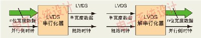
Figure 3: Word order is not preserved.
The adjustment of word order is usually carried out by searching for training codes. Some standard protocols usually define special code patterns for word alignment processing. For example, the main function of the K28.5 code pattern in 8B / 10B encoding is word alignment processing. The sending end inserts the K28.5 code pattern into the valid data, and the receiving end searches for the K28.5 code pattern in the received data. After finding it, the correct parallel data output is obtained by using this code pattern as a reference. In addition, protocols such as SDH use the A1A2 bytes of the frame header position for word alignment processing.
Other relatively low-speed LVDS interfaces also use low-frequency source-synchronous clocks to carry word alignment information in order to achieve correct data recovery at the receiving end. The low-frequency source synchronous clock here is also the follow-up clock in Figure 1. The multiple relationship between the LVDS data and the follow-up clock is usually equal to the multiple factor when the LVDS is serialized. For example, the Texas Instruments (TI) SN65LVDS95 LVDS transmitter can not only complete 21: 3 LVDS serial transmission, but also serialize 21-bit parallel data and clock into 3 LVDS data output and 1 clock output. The value of the serialization factor is equal to 7, so the frequency of the output clock is one-seventh of the LVDS data rate. Through this accompanying clock, the matching deserializer SN65LVDS96 can correctly restore parallel data. Compared with such separate LVDS SERDES devices, FPGA integrated LVDS modules can provide a higher degree of integration, and simplify hardware design, save PCB area, thereby reducing application costs. High-end FPGAs also solidify LVDS serializers / deserializers in I / O units to support very high rates, such as Altera's StraTIx III series.
The StraTIx III FPGA series is Altera's high-end FPGA based on the TSMC 65nm process. It is the industry's lowest power consumption product series with high-density and high-performance programmable logic devices. StraTIx III devices can simultaneously provide up to 276 pairs of LVDS serialized transmit modules and 276 pairs of LVDS deserialized receive modules. Each LVDS can support up to 1.6Gbps. In addition, it also exclusively provides programmable output swing and pre-emphasis to support long-distance backplane transmission, as shown in Figure 4. 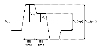
Figure 4: Stratix III supports programmable output swing (Vs (pp)) and pre-emphasis (Vpp (pp)).
Figure 5 shows the modules cured in the I / O unit in the Stratix III LVDS receiver. The source-synchronized low-frequency clock rx_inclk obtains DIFFI / OCLK after PLL frequency multiplication and phase shift, and samples the input data rx_in. The sampled data can be deserialized with a maximum factor of 10. 
Figure 5: Stratix III I / O cured LVDS receiver.
Due to the very high flexibility of FPGAs, such as supporting the frequency multiplication relationship between different LVDS input data and input clocks, and different deserialization factors, the output word order of Stratix III LVDS hard core modules is usually uncertain The word sequence may change after power-on or reset, and the word alignment needs to be performed according to the special pattern when using.
When the multiple relationship between the data input to the FPGA and the clock is equal to the deserialization factor of the deserializer, the FPGA has a certain word order output like a single LVDS deserializer, which can be used without training patterns Continue to apply normally. 6 is a timing chart when the deserialization factor is 7. Assuming that the rising edge of the accompanying clock corresponds to the highest bit of the data, within the FPGA, the PLL will generate a 7-times frequency sampling clock with phase adjustment from the accompanying clock. This clock samples the input data and sends it to the deserializer. By controlling the phase of the deserializer's loading clock, the determined parallel data output word order is obtained. The fixed difference between the phase of the loaded clock and the phase of the accompanying clock is achieved by receiving the phase control of the PLL, so the PLL reset control must be released after the input clock is stable, or the PLL is reset once the input clock is stable, otherwise the output The word order may not be fixed every time the power is turned on. 
Figure 6: Timing diagram of LVDS reception and deserialization.
In specific applications, it is also necessary to determine the word output sequence under specific applications through simulation, and then make adjustments in the logic design to make the final parallel output meet the needs. The specific design method and steps will be introduced as an example of interfacing with TI's SN65LVDS95 LVDS transmitter. This can also be used as a reference when connecting Stratix III LVDS to other LVDS devices. 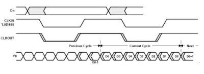
Figure 7: LVDS95 output timing. 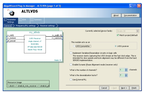
Figure 8: Comprehensive settings page.
Assuming that the clock frequency on the parallel side is 60MHz, the serial LVDS rate is 480Mbps. For the convenience of description, only one LVDS data is designed here.
First, the LVDS module (ALTLVDS) in Stratix III is called according to the timing of LVDS95. 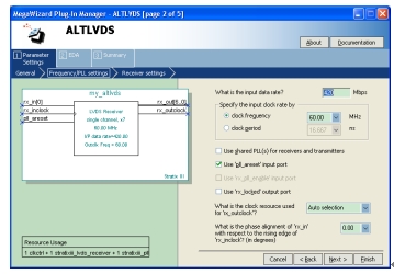
Figure 9: Frequency and PLL settings page.
In the integrated settings page of Figure 8, we did not select "Implement Serializer / Deserializer circuitry in logic cells", so we used the LVDS SERDES hard core. Also did not select the "Enable Dynamic Phase Alignment mode" option, which means that the DPA function is not used. 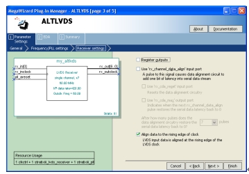
Figure 10: Receiver settings page.
In Figure 9, according to the output timing of LVDS95, 0 degrees is selected in "What is the phase alignment of 'rx_in' with respect to the rising edge of 'rx_inclock'?" In the setup in Figure 10, you usually need to select the "Register outputs" option. But because the subsequent design logic includes these registers, this option is selected here. In addition, the "rx_channel_data_align" port is not enabled here for word realignment. Next, we need to find out the word order of the LVDS hard core when the serial factor is equal to 7 through simulation. Figure 11 gives an example of the top-level design, and Figure 12 shows the simulation results in MODELSIM. 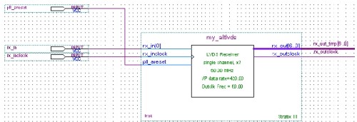
Figure 11: Design of the top-level module.
It can be seen from the simulation waveform in FIG. 11 that the first data after the rising edge of the LVDS clock will appear in rx_out_tmp [2] in rx_out_tmp [6: 0] on the parallel side. Combined with the characteristics of LVDS95, the MSB (D6) output by LVDS95 will appear in rx_out_tmp [0], so you need to slide this output by one bit to get the correct word order. 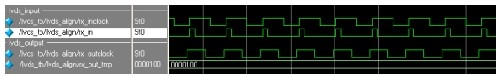
Figure 12: Simulation waveform.
In Figure 13, the data is first delayed by one beat to get rx_out_tmp_dly [6: 0], then rx_out_tmp_dly [0] is placed in the highest bit of the output data, and rx_out_tmp [6: 1] is placed on other bits in sequence to get The effect of sliding the data one bit to the right. If you need to slide multiple positions, adjust the above placement. We can further verify the above adjustment logic through simulation. Here we entered a counter data to confirm. Figure 14 shows the partial output of the simulation. In the figure, the two vertical bars on the left mark the "000001" data input by the LVDS, and the two vertical bars on the right mark the correct output of rx_out. This proves that our adjustment is correct. 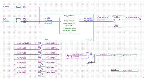
Figure 13: Word order adjustment logic. 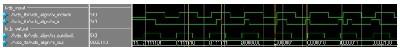
Figure 14: The simulated output waveform of the counter.
When using Stratix III for LVDS reception, we can set the deserialization factor to be equal to the multiple relationship between the input LVDS data and the clock, so that the determined word output order can be obtained, so that it can be implemented independently of the training code LVDS received word alignment. This method is not only suitable for FPGA to be connected with a separate LVDS transmitter, but also for data transmission between FPGA and FPGA. When used, the LVDS transmitter of the FPGA sends out a low-frequency source synchronous clock.