How to boost battery voltage in white LED applications
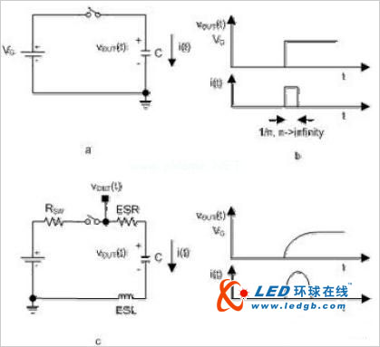
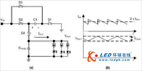
White LEDs are typically driven by a constant DC current source to maintain a constant brightness. In portable applications powered by a single Li-Ion battery, the sum of the voltage drops across the white LED and the current source can be higher or lower than the battery voltage, which means that the white LED needs to boost the battery voltage at some point. The best way to accomplish this is to use a step-up DC-DC converter. This approach can greatly optimize efficiency, but at the cost of increased cost and PCB area. Another way to boost the battery voltage is to use a charge pump, also known as a switched capacitor converter. This article will analyze in detail how this device works. The basic principle of charge pump A capacitor is a component that stores charge or electrical energy and releases it at a predetermined rate at a specified time. If an ideal capacitor is charged with the ideal voltage source VG (see Figure 1a), the charge will be stored immediately according to the Dirac current pulse function (Figure 1b). The total amount of charge stored is calculated as follows: Q=CVG The actual capacitor has an equivalent series impedance (ESR) and equivalent series inductance (ESL), neither of which affects the ability of the capacitor to store electrical energy. However, they have a large impact on the overall conversion efficiency of the switched capacitor voltage converter. The equivalent circuit for actual capacitor charging is shown in Figure 1c, where RSW is the resistance of the switch. The charge current path has a serial inductor that can be reduced by proper device layout design. Once the circuit is powered up, transient conditions of exponential characteristics are generated until a steady state condition is reached. The parasitic effects of the capacitor limit the peak charging current and increase the charge transfer time (Figure 1d). Therefore, the charge accumulation of the capacitor cannot be completed immediately, which means that the initial voltage change across the capacitor is zero. The charge pump takes advantage of this capacitive characteristic, as shown in Figure 2a. The voltage conversion is implemented in two phases. During the first phase, switches S1 and S2 are closed, switches S3 and S4 are open, and C1 is charged to the input voltage: In the second phase, switches S3 and S4 are closed and S1 and S2 are open. Because the voltage drop across the capacitor does not change immediately, the output voltage mutates to twice the input voltage value.. Using this method, voltage doubled voltage can be achieved. The duty cycle of the switching signal is typically 50%, which usually produces the best charge transfer efficiency. Let's take a closer look at how the charge transfer process and the switching capacitor converter parasitics affect its operation. The steady-state current and voltage waveforms of the switched capacitor voltage doubler are shown in Figure 2b. According to the principle of power conservation, the average input current is twice the output current. In the first phase, the charging current flows into C1. The initial value of the charging current is determined by the initial voltage across capacitor C1, the ESR of C1, and the resistance of the switch. After C1 is charged, the charging current decreases exponentially. The charging time constant is several times the switching period, and a smaller charging time constant will result in an increase in peak current. During this time, the output capacitor CHOLD provides the amount of linear discharge of the load current, and the amount of discharge is equal to: In the second phase, C1+ is connected to the output, and the discharge current (the current is the same as the previous charging current) flows through C1 to the load. At this stage, the output capacitor current changes by approximately 2IOUT. Although this current change should produce an output voltage change of 2IOUTESRC_HOLD, using a low ESR ceramic capacitor makes this change negligible. At this point, CHOLD is charged at the linear potential of the following battery: 
Figure 1. Charging the capacitor from a voltage source (Figures a and b are ideal, c and d are actual) 
Figure 2..a. Charge pump circuit, b. Related waveforms 


