Image video processing and display platform based on Zynq
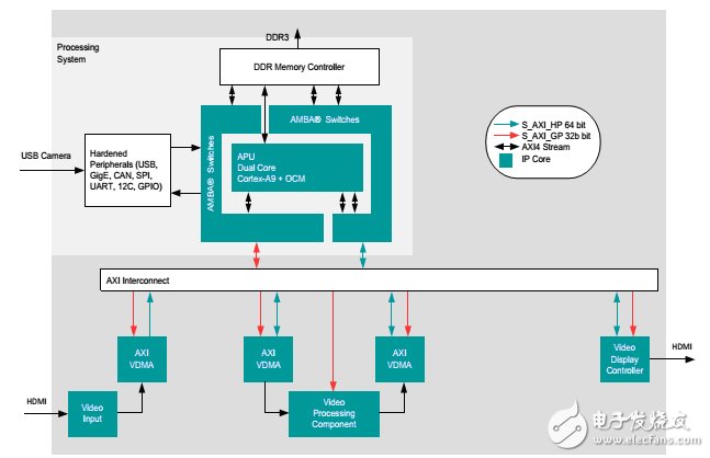
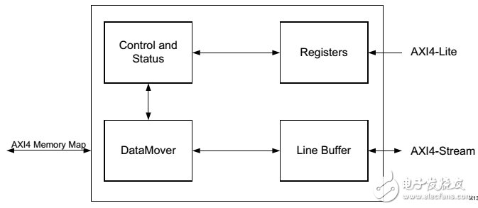
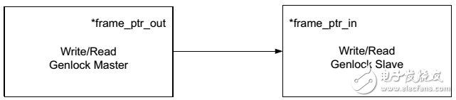
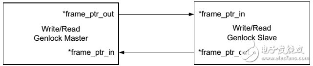
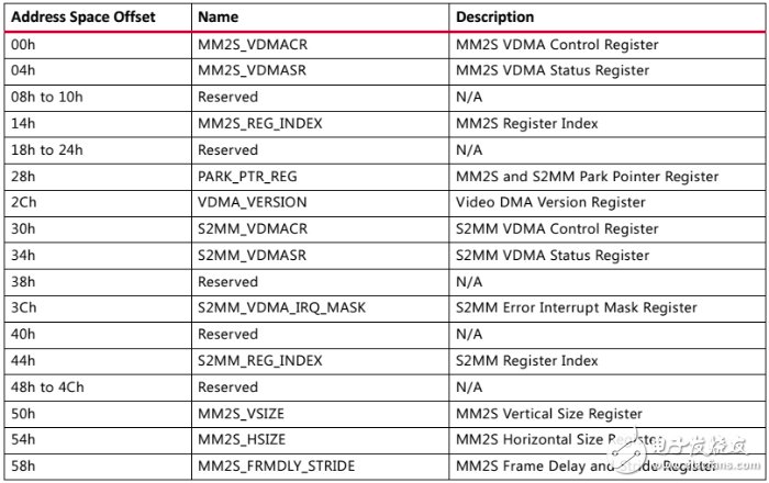
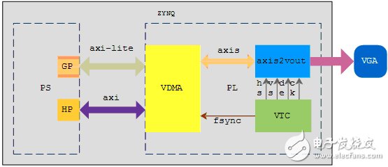
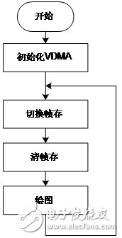
First, let's take a look at a structure diagram that often appears in the Xilinx ApplicaTIon Note. As shown in Figure 1, it is of course impossible for all the diagrams to be the same, and the structure is similar. This is a structural diagram of a typical image and video processing platform. 1.1, capture The video comes in through the HDMI interface, and then is formatted by the Video Input module and sent to VDMA. The function of the VDMA is to send the data into the frame memory opened in DDR3. The other is to obtain a video source through a device such as a camera, and send the data to DDR3 via PS/PL. At my current level, the easiest way for individuals to send video streams to DDR3 from the PL part is through the VDMA axi4-stream interface. In other words, converting the video stream to axi4-stream will reduce the processing difficulty. The conversion and the work of the Video Input module are similar. 1.2, processing This part contains two VDMAs and one video processing module. One VDMA is responsible for taking data from the frame memory and then handing it to the processing module. The processed result is sent back to the frame via another VDMA. 1.3, display Mainly the display control module, responsible for sending data to the display in accordance with standard timing output. Figure 1 video processing, display platform architecture As can be seen from Figure 1, the core of the entire architecture is the VDMA IP, so the key to building a platform is to master the use of VDMA. 2.1, the basic situation Let's take a look at the block diagram of VDMA and learn about the basics of VDMA. Figure 2 VDMA block diagram As shown in Figure 2, there are three main interfaces of VDMA, namely AXI4 Memory Map, AXI4-Lite, and AXI4-Stream. AXI4-Lite: This interface is the most commonly used interface in detail, used to read and write VDMA internal registers, thus achieving VDMA control and state acquisition. AXI4-Stream: Write channel (s2mm): VDMA fetches data from the axis interface and writes it to the frame memory Read channel (mm2s): VDMA reads data from the frame memory and sends it to the axis interface output. AXI4 Memory Map: This interface manual does not address the specific role, in fact, this interface is used to operate DDR, connected to Zynq's HP interface through the interconnect module. 2.2, use method: This part is a bit like nonsense, just like other IPs. i, new construction Ii, new block design Iii. Open the IP Catalog, enter keywords to retrieve to VDMA, or find IP cores by category. Iv, double-click VDMA IP, add IP to block design v. Configure the parameters of the IP if necessary. 2.3, VDMA configuration For detailed parameter configuration of VDMA, please refer to pg020, Product Guide, here is a place that I think is more important. i, GenLock mode The genlock mode has 4 choices: Master, Slave, Dynamic Master, and Dynamic Slave. Choosing different modes has different requirements for the port connection of the module, so it should be noted here that changing the mode, the port connection should also be modified, as shown in Figure 3 and Figure 4. image 3 Figure 4 Ii, Line Buffer Depth If the Line Buffer setting is unreasonable, it will affect the display effect and even cause no display. Iii, about the clock When you first get started, it is recommended to unify the clocks of the three interfaces AXI4-Lite, AXI4, and AXI-Stream into pixel clocks. After getting started, you can try three interfaces to use different clocks. It should be noted that the clock of the AXI4 interface must be greater than or equal to the clock of the AXI-Stream interface, otherwise data loss will occur. 2.4, VDMA initialization process 1. Write control informaTIon to the channel VDMACR register (Offset 0x00 for MM2S and 0x30 for S2MM) to set interrupt enables if desired, and set VDMACR.RS=1 to start the AXI VDMA channel running. 2. Write valid video frame buffer start address to the channel START_ADDRESS register 1 to N where N equals Frame Buffers (Offset 0x5Cup to 0x98for MM2S and 0xACup to 0xE8for S2MM). Set the REG_INDEX register if required. 3. Write a valid Frame Delay (valid only for Genlock Slave) and Stride to the channel FRMDLY_STRIDE register (Offset 0x58for MM2S and 0xA8for S2MM). 4. Write a valid Horizontal Size to the channel HSIZE register (Offset 0x54for MM2S and 0xA4for S2MM). 5. Write a valid VerTIcal Size to the channel VSIZE register (Offset 0x50for MM2S and 0xA0for S2MM). This starts the channel transferring video data. The function of the above registers can be found in Figure 5. For the function of each bit of a register, please refer to pg020, VDMA Product Guide, Chapter 2 Product SpecificaTIon Register Space. Figure 5 VDMA register offset address and role 3.1, logic design With the above-mentioned preparations, I believe that it is not very difficult to build a display platform. Below, I will give a concrete block diagram, as shown in Figure 6. (I originally wanted to use the top-level block design screenshots, found that the IP layout, the connection is messy, can not see clearly). In addition, you can also refer to xapp792, the same is true, my previous blog also mentioned how to build HDMI display platform, but recently there are users asking how to build a platform. In fact, the information given by the official website is often very informative, and everyone can pay more attention. Figure 6 Logic design example This is a graphics drawing and display platform, not a video processing platform, the video processing platform is slightly different. In general, video processing is not the same as genlock. All the signals and connections in the figure are the same as the actual design, which can reflect the design ideas. Vdma, axis2vout, vtc are three IPs, Vivado is provided, of course, you can also design yourself, the difficulty is not big, not to mention here. 3.2, software design The software flow chart is as follows: Figure 7 software flow chart It can be seen from the flow chart that the software part is very simple, because the display is responsible for the PL, the intersection of the two is stored in the frame, and the reading and writing does not conflict. The display picture read by the current PL is always the content of the previous frame drawn by the PS. If you want to reduce the PS burden, you can leave the task of clearing the frame to the PL. KNBL1-32 Residual Current Circuit Breaker With Over Load Protection
KNBL1-32 TWO FUNCTION : MCB AND RCCB FUNCTIONS
leakage breaker is suitable for the leakage protection of the line of AC 50/60Hz, rated voltage single phase 240V, rated current up to 63A. When there is human electricity shock or if the leakage current of the line exceeds the prescribed value, it will automatically cut off the power within 0.1s to protect human safety and prevent the accident due to the current leakage.
KNBL1-32 Residual Current Circuit Breaker,Residual Current Circuit Breaker with Over Load Protection 1p,Residual Current Circuit Breaker with Over Load Protection 2p Wenzhou Korlen Electric Appliances Co., Ltd. , https://www.korlen-electric.com
leakage breaker can protect against overload and short-circuit. It can be used to protect the line from being overloaded and short-circuited as wellas infrequent changeover of the line in normal situation. It complies with standard of IEC/EN61009-1 and GB16917.1.