How to use SPICE to simulate high-precision digital-to-analog converters?
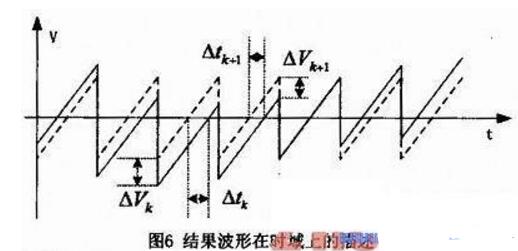
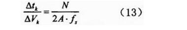
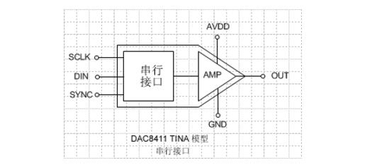
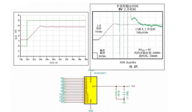
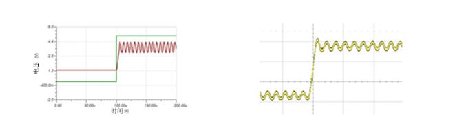
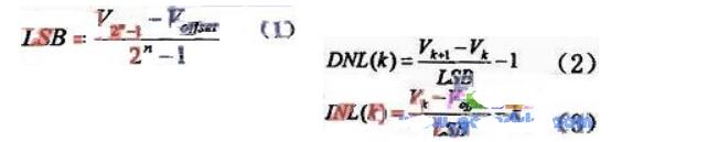
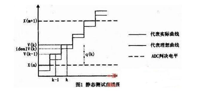
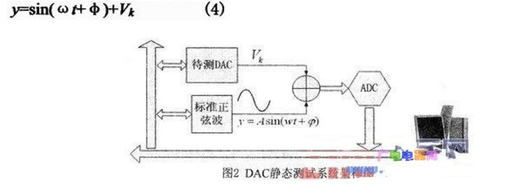
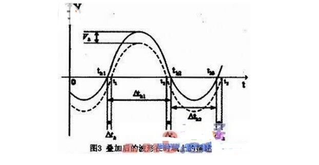
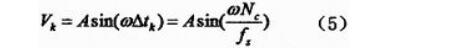
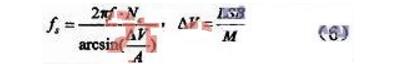
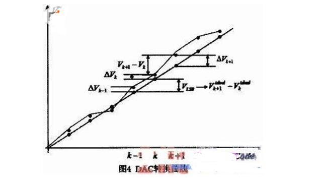
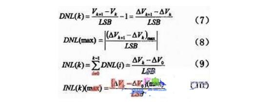
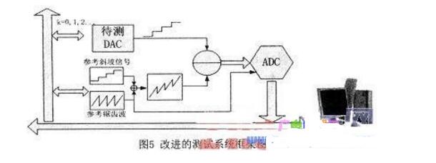
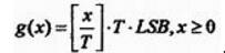
In this article, we will focus on system performance prediction and how to avoid design failures. The term that can be immediately reflected in Xiao Bian's mind to avoid these failures is "simulation". Currently, in addition to digital-to-analog converters (DACs), users can model and simulate most of the analog signal chain components in the SPICE simulation tool. With the SPICE model for high-accuracy DACs, board engineers no longer need to rely entirely on hand calculations before implementing actual hardware. We can provide two different SPICE models. One of them uses a simple n-bit wide parallel interface, as shown in Figure 1. This model is compatible with all TINA-TI version devices. The other model uses a serial SPI interface, as shown in Figure 2, which is compatible with industrial TINA-TI devices. Two different models include important dc characteristics for DACs and output amplifiers such as offset error, gain error, output voltage to power rail swing, temperature drift, and quiescent current. Other AC parameter characteristics include slew rate, settling time, power glitches, and stability. The SPI interface model also fully duplicates the digital interface and can be used to simulate the digital signal chain to the DAC input. Figure 1 - DAC8411 Model (Parallel) Figure 2 - DAC8411 Model (Serial) Predicting and inferring how a DAC or op amp behaves when driving a specific load is an important aspect of any design. Let's look at an example. In this example we use the DAC8411SPICE model to simulate the settling time. The left side of Figure 3 shows the transient simulation of the DAC output. The code step is from 1â„4 full scale to 3â„4 full scale. In this simulation, the DAC is driving a 2kΩ resistive load in parallel with a 200pF capacitor - the same load is used to specify the settling time in the datasheet. The SPICE model accurately replicates the settling time of typical characteristic curves in the data table shown on the right side of FIG. Figure 3 - DAC8411 Transient Simulation But what if you are driving a different load than the load specified in the data table? The left side of Figure 4 shows a simulation. In this simulation, a larger value of 20nF capacitive load is applied to the DAC output. In this case, transient simulations show that there is considerable ringing, or oscillation, at the DAC output due to the instability of the output amplifier with large capacitive loads on it. The complete SPICE model provided helps to catch such problems earlier, so that compensation components can be included in the design of the first prototype. Figure 4 - Transient Simulation with DAC841120nF Capacitive Load In summary, the latest SPICE model for high-accuracy DACs is designed to provide engineers and designers with a unique way to simulate the entire analog signal chain, identify problems early, and shorten time-to-market. The following two TI high-precision designs allow you to dynamically learn about the new DACSPICE model: 1. TIPD158 - Low Cost Loop-Powered 4-20mA Transmitter Electromagnetic Compatibility/Electromagnetic Interference (EMC/EMI) Performance Tested 2. TIPD160 - State Variable Filter Based on Digitally Adjustable Multiplier Digital-to-Analog Converter (MDAC) For the DAC static test, the two parameter values ​​of DNL and INL are usually tested by entering the code k, k=0, 1, 2...2n-1. The DAC output level value Vk is obtained. The formulas for calculating DNL and INL are as follows: If we directly test it with an ADC with lower precision than the DAC, as shown in Figure 1, we cannot distinguish the exact voltage values ​​corresponding to the input codes k and k-1 due to the quantization error q(k) introduced by the low-accuracy ADC. The static parameter test in this case loses its meaning. The zero-crossing detection method is a classical modulation domain analysis method. It can obtain the zero-crossing time interval by recording the zero-crossing time and can be used to identify weak signals with an accuracy lower than the ADC step size. Figure 2 briefly describes the test system block diagram: the voltage Vk of the DAC to be measured, the calibrator provides a standard reference sine wave f(t) = Asin(ωt + φ), the DC voltage Vk is added to the reference sine wave, The resulting signal is input to a high speed ADC. which is: The performance of Equation (4) on the time domain graph is shown in Figure 3. In the figure, the dotted line represents the standard reference signal f(t) = Asin(ωt + φ), and the solid line is the signal after superposition. It can be seen that tk1, tk2, tk3 are zero-crossing points, and the size of Vk is determined by Δtk. The value of Δtk can be obtained by measuring the zero crossings tk1, tk2, tk3. The expression of Vk can be derived as follows: Among them, Nc is the number of sampling points in the interval Δtk, and fs is the sampling rate of the set ADC. Using the above method, the value of the DAC output voltage Vk can be obtained, and the static parameters DNL and INL can be obtained. It is necessary to pay attention: in order to get the zero-crossing sequence, the amplitude A of the reference sine wave must be greater than the full-scale voltage range of the DAC; the lowest sampling rate of the ADC is given by (5): The ΔV amplitude resolution can be seen from equation (6): To ensure the accuracy of the test, ΔV should be as small as possible, and the value of Nc should be larger with other conditions unchanged. Because the essence of this method is to shift the high-precision test in amplitude to the time. Therefore, the higher the sampling rate, the more accurate the measurement results, but the sampling rate is closely related to the test equipment, and it is impossible to increase without limit. In this case, if no device can provide a sufficiently high sampling rate, only the signal frequency f can be reduced. However, reducing the signal frequency f will bring another problem, that is, the test time will increase exponentially. In the literature, the authors measured 16-bit DACs with an amplitude of ±10V and used a Tektronix TDS7404B digital oscilloscope as the ADC for the acquisition of signals. Its main parameters are: 8-bit resolution, the highest sampling rate of 20GS/s. Set ΔV=LSB/40, Nc=5, sine wave frequency f=100Hz, amplitude A=11V. The sampling rate obtained by Equation (6) is as high as 5 GS/s. Measure 10 VKs at a time to average them. This takes 0.1s per Vk to be measured. Even with such an ultra-high sample rate device, the time required to completely measure a 16-bit DAC requires at least Two hours. From the perspective of reducing the test time: First of all, from Figure 3, we can see that using a sine wave as a reference waveform requires at least 3 zero-crossings to obtain the output voltage value of the DAC, and secondly, to reduce the need for detecting each zero-crossing point. The most direct method is to increase the frequency f of the reference signal, but the sampling rate fs cannot be increased due to the limitation of the device conditions. From equation (6), it can be seen that Nc and ΔV are convention values ​​and cannot be changed. The only thing that can be changed is the reference sine wave amplitude A, but the minimum value of A is also limited because A is smaller than the tested DAC. In the measurement range, the output voltage greater than A in the DAC cannot be measured. In fact, the limitation of A is because we need to test the output voltage value of each code. But in fact, we don't need to test every Vk. For static testing, the main thing to understand is the linearity of the DAC under test, as shown in Figure 4. The main influence on DNL is the difference between the difference between the output levels of two adjacent input codes and the ideal step, that is, the difference between Vk+1-Vk and LSB. Change the formulas for DNL and INL as follows: From Fig. 4 and Eqs. (7) and (9), it can be seen that the static parameters of the DAC can be calculated as long as the difference between the actual voltage of the input code and the ideal voltage is known. Based on the above understanding, the following test system architecture model was designed. Set the reference sawtooth signal The reference ramp signal can be expressed as: Let the signal generated by the DUT be g'(x), and the sawtooth signal with the uniform jitter increased by superposition is f(x)*δT(x)+g(x). The signal acquired by the ADC is f(x)*δT(x )+g(x)-g'(x). Obviously, the value of g(x)-g'(x) represents the magnitude of ΔVk, while ΔVk is very small, which cannot be reflected by the low-accuracy ADC. It can be expressed by the zero crossing of the reference sawtooth waveform in the time domain. If the DAC under test exhibits perfect static characteristics, the ADC will recover the reference sawtooth signal. If the output voltage Vk of the tested DAC deviates from the ideal value (as shown in Figure 4), it will be clearly visible in the time domain diagram. Reflected, as shown in Figure 6. In the figure, ΔVk represents the difference between the actual measured level and the ideal level at this point when the input code is k. The dotted line represents the reference sawtooth signal, and the solid line represents the differential signal between the measured DAC and the reference signal. With a dual-channel ADC, the two signals are collected at the same time. By detecting zero-crossings, the values ​​of Δtk and Δtk+1 are obtained. It is easy to see that: N represents the sampling point in one cycle of the sawtooth wave, A represents the amplitude of the sawtooth wave, and then there is: The result proves that in the above method, knowing the amplitude of the sawtooth wave and the number of sampling points Nc in Δtk, the value of Δtk can be obtained. In this method, it is not necessary to know the value of each Vk, and it is also easy. Obtain the values ​​of DNL and INL. In order to verify the reliability of this method, Labview virtual instrument was used for simulation test. The 8-bit DAC is used in the simulation to generate the standard ramp and sawtooth waveforms. The addition of the two signals is used as the reference waveform. The random white noise point is added point by point to the standard ramp waveform, limiting the LSB range to use the program. Calculate the actual simulated DNL and INL size. The ultimate goal of the program is to compare the results of the proposed method test with the actual calculation results. By writing a test program, you can get the following rules: (1) The higher the sampling rate of the ADC, the more DNL and INL obtained by the actual test will be closer to the actual calculation result; (2) The smaller the reference sawtooth amplitude, the more accurate the test result will be; (3) The number of ADC bits has little to do with the accuracy of the test. It should be noted that increasing the number of sampling points will increase the test time, so the ADC sampling rate can not be increased without limit, but it can be best evaluated based on the actual situation of the test. With regard to the setting of the amplitude, the lowest value must have zero crossings for each differential sawtooth wave. Then set the program to compare the zero crossing of the standard sawtooth wave with the number of zero crossings of the differential sawtooth wave. When the two are different, the lamp in the program will alarm. In the simulation test, set the DAC range to 10V and the amplitude to 80mV. In the generated ramp, each input code is repeated 100 times. The sampling rate is set to 1k and 256000 points are collected. Set the resolution of the ADC to 2 bits. The result is shown in Figure 6. Comparing the number of samples between the zero crossings of the two waveforms in Figure 6, compare the resulting INL value with the calculated INL value: Figure 7a. The actual INL value, b. The INL value measured by this method. This paper presents a new evaluation method for dynamic testing of high-accuracy DACs. This method obtains the values ​​of the static parameters INT and DNL of the DAC accurately by comparing the saw-tooth wave with the actual zero-crossings of the sawtooth wave in the time domain. And verified in Labview simulation test system, the result proves the effectiveness and practicability of this method. Patch Panel,48 ports patch panel,half U patch panel,patch panel 24 port NINGBO UONICORE ELECTRONICS CO., LTD , https://www.uniconmelectronics.com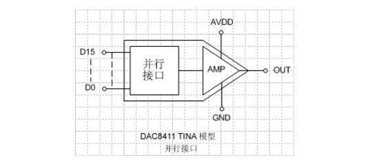
 ,among them:
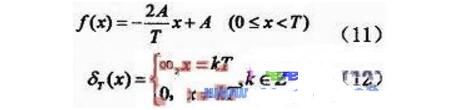
 , [] is a rounding function.