TLK3132 working principle CPRI interface application (2)
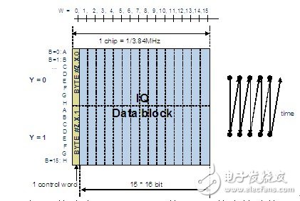
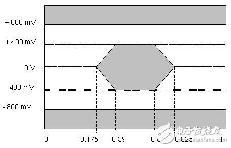
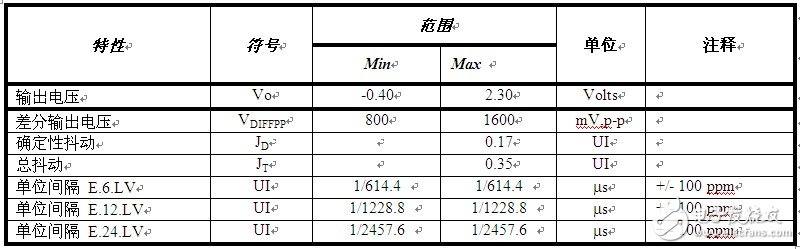
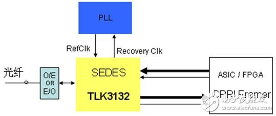
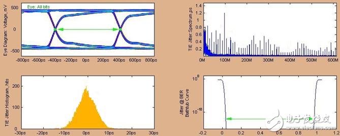
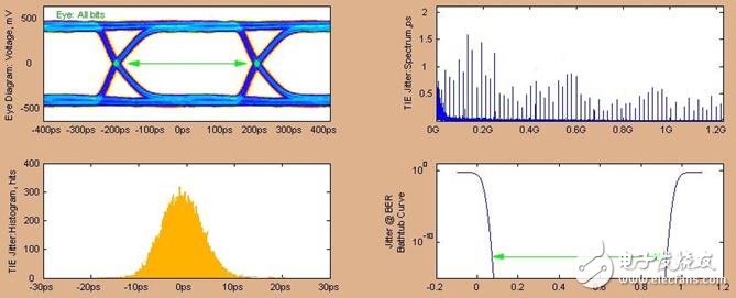
In order to deal with the fiber link of the baseband unit and the radio frequency unit in the RF module remote technology, two standardization organizations have been established internationally: one is CPRI (Common Public Radio Interface), which was initiated by Huawei, Ericsson, NEC, Siemens and Nortel in 2003. Established organization dedicated to the standardization of baseband and RF interfaces; the other is OBSAI (Open Base StaTIon Architecture IniTIaTIve), an alliance established by Nokia, LG Electronics, Samsung Electronics, etc. Both define a standardized interface for separating the baseband from the radio frequency, that is, the macro base station is divided into two parts: a baseband unit BBU and a remote radio unit RRU, and the I/Q data and control management data are transmitted between the BBU and the RRU, and the signals thereof The format is the standard interface defined by CPRI or OBSAI. This article takes the CPRI interface as an example to explain the application of TLK3132 in the remote sensing technology of RF modules. 1.1 CPRI interface The CPRI interface defines a physical layer layer1 and a data link layer layer2 protocol in the transport user interface. In the physical layer, serial/parallel conversion of the data of the upper access point and codec of the physical layer (the CPRI interface is recommended to adopt 8B/10B, following the IEEE 802.3 2005 Clause36 recommendation); at the data link layer, The upper access point's I/Q data, physical layer protocol data, network protocol data (including Ethernet data, high-level data link protocol data), and vendor-defined control information are processed accordingly. Currently, CPRI has three recommended link rates, which are 614.4 Mbps, 1228.8 Mbps, and 2457.6 Mbp. On the transmitting side, I/Q data, control protocol information, synchronization information, etc. are multiplexed into CPRI frame structure information, and after 8B/10B encoding of the physical layer, long-distance propagation through optical fibers (several kilometers to tens of kilometers); On the receiving side, the CPRI frame signal is serially converted and then decoded into corresponding I/Q data and control protocol information through 8B/10, and processed by the upper layer data link. The CPRI frame is divided into a basic frame unit and a super frame unit. The frame rate of the basic frame unit is 3.84MHz, including 16 words (represented as W=0...15, where W0 is the control word and the last 15 words are I/Q data). The length of the word is according to different link rates. They are 8bits, 16bits (as shown in Figure 7) and 32bits. The superframe unit is composed of 256 basic frame units, wherein the control word in the first basic frame unit is written with the K28.5 flag as the synchronization control information of the superframe, and the control words in the remaining 255 basic frame units are included. Control and management words (C&M), vendor-defined control words, etc., and reserve some control words. Figure 7 CPRI basic frame structure with line rate of 1228.8Mbps In high-speed data link communications, jitter specifications are critical, and the CPRI interface recommends eye diagram and jitter specifications for high-speed serial signals. On the SERDES sending side, the eye pattern template required by CPRI is shown in Figure 8. Figure 8 CPRI interface send output eye diagram template (ExLV) Table 1 E.6.LV, E.12.LV and E.24.LV Transmitter AC Timing Specifications (Reference CPRI SpecificaTIon V2.0) In the implementation of the CPRI interface, the TLK3132 performs high-performance serial/parallel, parallel/serial conversion, and synchronization of CPRI frames and 8B/10B codec, that is, the relevant functions of the physical layer of the CPRI interface. 1.2 Application examples According to the previous TLK3132 device characteristics analysis and CPRI interface introduction, TLK3132 can meet the application requirements of CPRI interface well. Figure 8 is a typical functional block diagram of TLK3132 in CPRI link: TLK3132 receives high-speed serial from photoelectric conversion After the serial signal is converted, the corresponding control characters and valid characters are extracted and 8B/10B decoded, and then sent to the ASIC or FPGA for CPRI deframe processing; meanwhile, the CPRI frame signal from the ASIC/FPGA is also received, and corresponding The 8B/10B code is sent to the SERDES Core for serial and serial conversion. In this circuit, the TLK3132 restores the clock to the PLL as a reference clock, and its reference clock comes from the output clock of the PLL. In order to ensure the reliable operation of the internal CDR, the TLK3132 requires that the reference clock and the input high-speed serial data have a frequency offset of +/-200PPM. Therefore, in the case of loss of the peripheral PLL, the free oscillation frequency of the local oscillator must be stable enough. A clock scheme based on a voltage controlled crystal is generally recommended. Figure 8 Typical application of TLK3132 on CPRI interface The following example shows how to set up the software configuration of the TLK3132 related registers via MDIO. Assume that the serial rate of CH0 and CH1 channels are 1228.8Mbps and 2457.6Mbps respectively, the parallel interface uses SDR interface and works in NBI mode, enables internal 8B/10B codec, differential reference input 122.888MHz clock, internal jitter filter lock When the phase loop is closed, the reference software configuration on TI's TLK3132 evaluation board is as follows. START CLAUSE 22 //Select CLAUSE 22 mode SETPHYADD(00) //Select physical address 0 WRITE (00, 8000) / / software reset chip, that is, reset all registers READ(11, 3590, FFFF) // Verify that the MDIO function is normal WRITE(1E, 9100) //Write 0x3FF0 to the 0x9100 register and the differential reference input as the reference clock for the SERDES Core WRITE (1F, 3FF0) WRITE (1E, 9000) //The frequency multiplication factor of the high frequency multiplier is set to 10 WRITE (1F, 1515) WRITE (1E, 9001) //Set CH0 to 1/2 speed - 1228.8Mbps, CH1 to full speed - 2457.6Mbps WRITE (1F, 6060) WRITE (10, 8400) / / parallel receive clock to select the recovery clock of the respective channel WRITE (11, B197) //The parallel port is SDR and works in NBI mode, rising edge data, 8B/10B enable WRITE(1E, 9002) //Set CH0 channel reception as AC coupling, adaptive equalization WRITE (1F, 1005) WRITE(1E, 9004) //Set CH1 channel reception as AC coupling, adaptive equalization WRITE (1F, 1005) WRITE (1E, 900A) //Set the CH0 channel serial transmitter to swing at 1000mV and de-emphasize to 9.52% (0.87dB) WRITE (1F, 0B21) WRITE (1E, 900C) //Set the CH1 channel serial transmitter to swing at 1000mV and de-emphasize to 9.52% (0.87dB) WRITE (1F, 0B21) WRITE (10, 8C00) / / data channel reset PAUSE (100) / / Wait for the chip configuration to take effect WRITE (1E, 901B) / / Check if the internal phase locked loop of the SERDES Core is locked READ(1F, 0011, 0011) STOP 1.3 Experimental test Since the serial port rate is as high as 1228.8 Mbps and 2457.6 Mbps, it poses a big challenge to the layout of the PCB. At the same time, the TLK3132 has excellent loss compensation capability and can adjust the optimal de-emphasis compensation level for optimal signal integrity performance. In the example in Section 3.2, K28.5 bytes of data are repeatedly sent. The actual eye diagram of the TLK3132 transmitter is shown in Figure 9 and Figure 10 (the corresponding serial rates are 1228.8Mbps and 2457.6Mbps respectively). The jitter is mainly derived from Random noise, eye width is above 0.9 UI, with very good jitter performance (compensate the loss of transmission line FR4 by appropriately adjusting the de-emphasis ability to improve SI performance). Figure 9 1228.8Mbps transmission side eye diagram (with 5inches FR4 routing, adjusted for optimal de-emphasis compensation) Figure 10 2457.6Mbps transmission side eye diagram (with 5inches FR4 routing, adjusted for optimal de-emphasis The TLK3132 is a low-power, low-jitter, low-cost, high-performance multi-rate transceiver with flexible internal module configuration that makes it widely used in high-speed serial communications. In order to reduce the networking cost and improve coverage of wireless networks, RF remote technology is widely used in 3G network construction. The baseband unit and RF unit in the original base station can be separated through standardized interfaces (such as CPRI) to reach a computer room. Network layout of multiple antenna configurations to reduce operator investment in fixed equipment rooms. As a key technology implemented by the CPRI interface - high-speed serial-parallel / parallel-serial transceiver, TLK3132 provides very superior SI performance, standard 8B/10B and channel synchronization processing, flexible on-chip clock generation and distribution, etc. Reliable, multi-rate CPRI interface standard requirements. Puff Bar,Puff Bar Vape,Disposable Vape Puff Bar,Vape Pen Puff Bar Nanning Nuoxin Technology Co., LTD , https://www.nx-vapes.com