BUCK power circuit design test process sharing
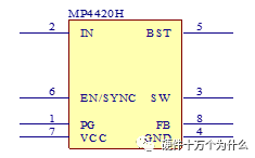
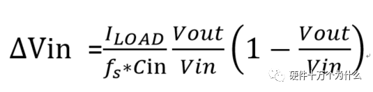
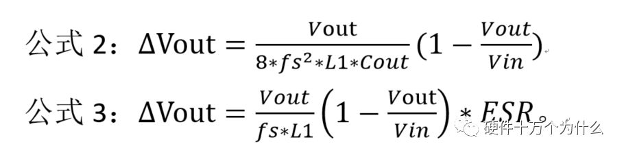
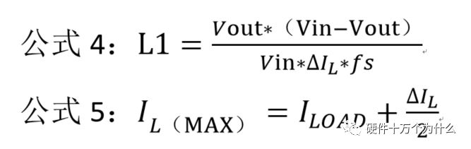
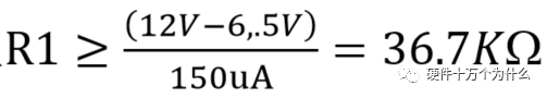
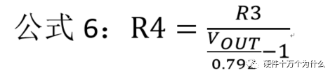
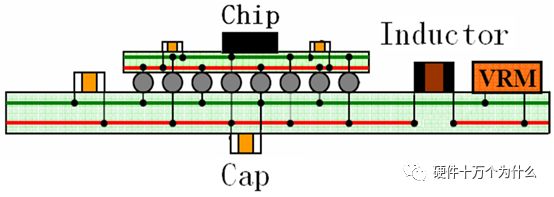
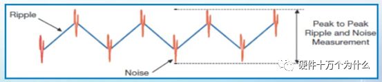
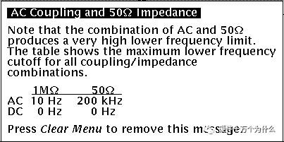
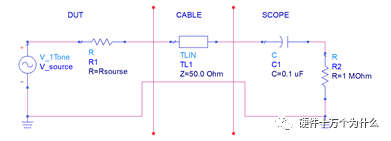
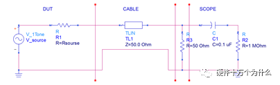
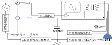
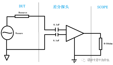
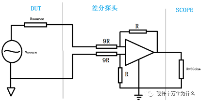
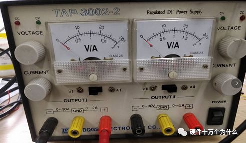
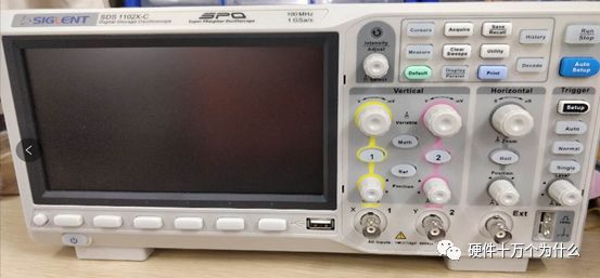
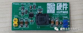
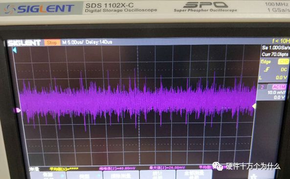
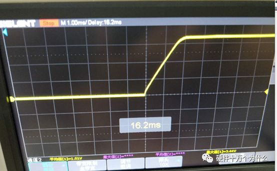
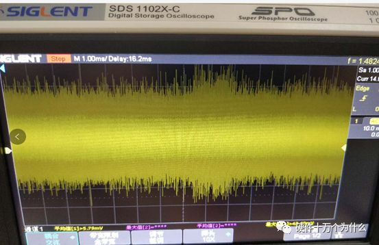
1 chip selection Figure 1 shows the schematic circuit diagram of this module, which can be simplified as input part, control part, output part and feedback part. Input part: Capacitance C1, C2, C3, and R1; Control part: MP4420H chip and bootstrap circuit C5, R5; Output part: Inductor L1, Capacitance C6, C7, and C8. Feedback section: Resistors R3, R4, and R2. Figure 1 Power module schematic This module needs to implement a DC-DC power conversion function with an input of 12V and an output of 3.3V/2A. Select MP4420H this chip, MP4420H input range is between 4V-36V, the output voltage range is 0.8V-32.4V, the maximum output current of 2A. The characteristics of the MP4420H include: Built-in two switch tubes with synchronous BUCK technology, switching frequency of 450KHz, internal soft start, duty cycle up to 95%, and thermal shutdown. Figure 2 shows the pin diagram. Figure 2 MPH4420H pin diagram PG: The output of this pin is open drain, the output voltage is high 90% of the nominal voltage IN: power input, generally connected with several capacitors for energy storage and decoupling SW: Switch output pin GND: Ground BST: On the bootstrap pin, a capacitor must be connected between the SW and BST pins to form a floating voltage to drive the upper switch of the MP4420H. The bootstrap capacitor recommends connecting a 20-ohm resistor in series to reduce the SW peak voltage. EN/SYNC: Enable/Sync pin VCC: Bias voltage, usually a decoupling capacitor of 0.1Uf ~0.22uF, no more than 0.22uF FB:Feedback 2 capacitor selection 2.1 Input Capacitor Selection: The main purpose of the input capacitor is energy storage and filtering, so as to prevent the external power supply module from supplying power when the output requires a large current, thereby causing the output voltage to drop. When selecting the input capacitor, first ensure that the voltage of the capacitor is 1.5 times the voltage of the power supply module. According to the data sheet of MP4420H, the input capacitance formula 1 can be known: Formula 1: For the output current 2A, fs is the switching frequency 450KHZ, Cin is the input capacitance, Vout is the output voltage 3.3V, and Vin is the input voltage 12V. This module uses the 22μF ceramic chip capacitor recommended in the MP4420H datasheet and can calculate 44mV. Choose two Fenghua brand 10uF/25V C1 and C2 ceramic chip capacitors in parallel, and then connect a small capacitor with a capacitor C3 size of 10nF/25V in parallel to filter out the high frequency signals in the input DC voltage. 2.2 Output Capacitor Selection: The value of the output filter capacitor can be obtained by calculation, but generally, when the capacitor value is selected, it usually selects 1.2-2 times the calculated capacitor value or larger capacitance. It is better to connect multiple capacitors in parallel under the condition that the PCB area allows. Because the output filter capacitor and the output inductor will form two poles, this will cause the circuit output to be abnormal. The specific performance is that the output ripple is large and the output rising edge has strong oscillation. Therefore, the inductor value must be properly considered when selecting the capacitor value. According to the MP4420H data sheet, the output capacitance is related to the following formula: L1 is the output filter inductor and ESR is the internal resistance of the output capacitor. Therefore, according to the output ripple requirements can be roughly obtained the size of the output capacitor, in the choice of capacitance when the capacitor will generally choose the larger point of capacitance. For a switching power supply module, the power supply itself generates a power supply ripple that is consistent with the switching frequency and is always superimposed on the power supply output. The output ripple is also caused by the internal resistance of the output capacitor, which continuously charges and discharges the output capacitor. The charging current will have a voltage drop across the output capacitor's internal resistance, ESR, and this will produce an output ripple. When choosing the output capacitor, try to select the smaller ESR ceramic capacitor instead of the electrolytic capacitor. Selecting several capacitors in parallel is also to reduce the output internal resistance. Generally, a small capacitor in parallel at the output is generally used to filter the nF capacitor. Go to high frequency ripple. This module selects two 100uF/16V and one 100nF/16V SMD ceramic capacitors in parallel. 3 inductor selection The main function of the output inductor is to stabilize the output current and energy storage. The LC filter circuit composed of output inductor and output capacitor is mainly used to smooth the output voltage so that the output voltage is a stable DC. When selecting the output inductor, in addition to considering the value of the inductor value, it is necessary to consider the current value that the inductor can suppress. The current rating of the output inductance of the BUCK switching converter is at least 1.2 times the output current. According to the data sheet of MP4420H, the inductance value of the output inductor is 1uH~10uF, and the inductor current rating is at least 25% of the load current. For most designs, the inductance value can be obtained by the following formula: The slope current for the inductor is typically 30% of the maximum inductor current. According to the calculation, the output inductor value is 8uH, and the 10uH/5A chip inductor is actually selected. 4 resistance selection Enabling the selection of resistor R1, the EN/SYNC pin is used to control whether the chip is working. When it is high, the chip is enabled; when it is low, the chip does not work. The EN/SYNC pin has a 6.5V regulator. Connecting an enable resistor to the input enables the circuit. The current flowing into the enable resistor is less than 150uA. Therefore, this module's enable resistor Select R1=100KW. The feedback part of the resistance selection, MP4420H external feedback resistor to form a closed-loop circuit, so that the output is stable at 3.3V. The feedback voltage is obtained through the partial pressure of R3 and R4. The feedback voltage is compared with the internal comparator of MP4420H. When the feedback voltage is greater than the reference voltage of the internal comparator 0.8V, the internal switch of the MP4420H is turned off to cut off the input to the output. . The size of recommended R3 in the data sheet is about 40KW, and 41.3KW is selected in this module. So you get R4: From Vout=3.3V, R4=13KW R3 and R2 are used to set the loop bandwidth. The larger R3 and R2 are, the smaller the bandwidth is, and the loop bandwidth is generally less than 1/10 of the switching frequency fs to stabilize the output. According to the data sheet, the recommended R2 is 51KW. Second, the power test 1 Power PDN and Ripple Noise 1.1 Power PDN The power supply ripple noise test is a more complex test problem. The results measured by different methods are different. Even if the test method differs from the same test method, the test results will generally differ. For terminal products, whether it is CPU, GPU, DDR, etc., there are thousands of transistors inside the chip. Different circuits in the chip need different power supply. Commonly there are Vcore, Vcpu, Vmem, VIO, Vgpu, Vpll. Such as these power supply DC-DC power supply module power supply, but also LDO power supply module power supply, are unified by the PMU to manage. As shown in Figure 3, for the PDN diagram of the chip, the power supply loop of the chip starts from the voltage regulator module VRM, to the power network of the PCB, the ball pin of the chip, the power network of the chip package, and finally reaches the die. When the chip works At different loads, the VRM cannot respond to the rapid change in current demand of the load in real time, causing a drop in the power supply voltage of the chip, thereby generating power supply noise. For the VRM of the switching power supply module, the power supply itself generates a power supply ripple that is consistent with the switching frequency and is always superimposed on the power supply output. For power supply noise, it is necessary to use decoupling capacitors on the package and PCB, design a reasonable power ground plane, and finally filter out power supply noise. For power supply ripple, you need to increase the BULK inductance or BULK capacitance. Figure 3 Schematic diagram of chip power distribution network (PDN) For board-level PCB design, when the frequency reaches a certain frequency, the high-frequency noise cannot be filtered out due to the effect of the ESL of the trace and the ESL of the capacitor. The industry believes that the PCB can only handle noise within 100MHz, and higher-frequency noise is required. Package or die to solve. Therefore, for board-level power supply noise tests, an oscilloscope with a bandwidth of 500M or more is sufficient. In general, the greater the bandwidth of the oscilloscope, the lower the noise will rise. Therefore, it is recommended that the bandwidth of the oscilloscope be limited to 1 GHz when testing the power supply. 1.2 Power Ripple and Power Supply Noise Power supply ripple and power supply noise is a relatively confusing concept. As shown in Figure 4 below, the blue waveform is the power supply ripple and the red waveform is the power supply noise. The frequency of the power supply ripple is the fundamental frequency and harmonics of the switching frequency, and the frequency content of the noise is higher than the ripple. It is the transient current generated by switching on-chip high-speed I/O switching, the parasitic inductance of the power supply network, and the power supply. Electromagnetic radiation between the plane and the ground plane and many other factors. Therefore, the output of the power supply is measured as ripple on the PMU side, and the power supply noise is measured on the SINK (power consumption chip, such as AP, EMMC, MODEM, etc.). Figure 4 Power Ripple Noise Figure When the power supply ripple is measured, the oscilloscope bandwidth is limited to 20MHz. The power supply ripple can be measured by measuring the peak-to-peak value of the PMU power output. After the design of the PMU chip is completed, the chip manufacturer will do a load test to test the ripple condition of the output power of the PMU under different loads. Therefore, in the terminal product board, there is no need to do the test in this respect. The ripple size refers to the PMU. Manual can be. In the power noise test, the test point is placed on the SINK pin. Since the working speed of the SINK pin is more than several tens of MHz, the oscilloscope bandwidth is set to the full band (up to the bandwidth limit of the oscilloscope), and the test point should be as close as possible to the power pin of the test chip. If there are multiple power supply pins, the one that is the farthest from the PMU should be selected. The power supply noise is related to PCB layout and location of the DECAP capacitor. At the same time, the power supply noise affects the CPU operating status and the EMI of the board. The terminal board needs to test the power supply noise of each board. 2 Common Ripple Noise Test Solutions 2.1 Ripple noise test basic requirements At present, the operating frequency of the chip is higher and higher, the operating voltage is getting lower and lower, the operating current is getting larger and larger, and the noise requirements are also more demanding. Take the CORE core of the MSM8974 as an example, the voltage is 0.9V, the current is 3A, and the requirement is 25MHz. The AC PDN impedance is 22mohm and the power supply noise requirement is within ±33mV. For DDR3 chips, VREF power supply noise is required to be within ±1%. If 1.5V power supply is used, the noise peak-to-peak value is not more than 30mV. This kind of low-noise power supply test is very challenging, and the main points that affect its measurement accuracy are as follows: (1) The noise floor of the oscilloscope channel; (2) The resolution of the oscilloscope (ADC's ADC digits); (3) The oscilloscope vertical scale minimum (quantization error); (4) Probe bandwidth; (5) The distance between the probe GND and the two test points of the signal; (6) Oscilloscope channel settings; When testing power supply noise, the following conditions are required: (1) It is necessary to test the power supply ripple under heavy load conditions; (2) CPU, GPU, DDR frequency should be locked at the highest frequency when testing power supply ripple; (3) The test point should be farthest from the PMU at the SINK end; (4) The test point should be close to the BALL of the chip; (5) Bandwidth is set to full frequency band; (6) Oscilloscope bandwidth is greater than 500MHz; (7) The noise waveform accounts for more than 2/3 of the entire screen or the vertical scale has been a minimum; (8) The shortest loop between the probe ground and the signal, minimum inductance; (9) The test time is greater than 1min, the sampling time is more than 1ms, and the sampling rate is 500Ms/s or more; (10) Ripple noise looks at the Pk-Pk value and focuses on the Max and Min values; 2.2 High-pass filter characteristic analysis The oscilloscope has two AC and DC coupling modes. When using AC coupling, its internal equivalent circuit is shown in Figure 5. C is the value of the capacitance, R is the impedance of the terminal to ground, Vi is the input signal, and Vo is the measurement signal. The cutoff frequency of the filter is when when when when Fig. 5 Equivalent circuit of high-pass filter after adding capacitance capacitor Table 1 Frequency points corresponding to different value capacitors 2.3 Passive Probe DC Coupling Test Passive probe DC coupling test, the oscilloscope is set to DC coupling, the coupling impedance is 1Mohm, then the passive probe's ground wire is connected to the motherboard ground, and the signal line receives the power signal. This measurement method can measure power supply noise ripple other than DC. As shown in Fig. 6, when an ordinary crocodile clip probe is used, the loop between the ground and the signal to be measured is too large, and the detection point of the probe is close to the IC chip running at a high speed, and the near-field radiation is large and there is a lot of EMI. Noise is radiated into the probe loop, making the test data inaccurate. To improve this situation, when using a passive probe to test the ripple, use the probe in the figure to ground the signal on the signal pin. This is equivalent to a loop inductance between ground and the signal. The signal is equivalent to high resistance, effectively suppressing high-frequency noise due to radiation. More often, it is recommended that the tester use a third test method to wrap an enameled wire around the probe, and then solder the enameled wire to the mainboard ground and move the probe to test each line of power supply ripple noise. At the same time passive probes require the use of 1:1 probes as much as possible, eliminating the use of 1:10 probes. Figure 6 Two methods of passive probe grounding For an oscilloscope, if the vertical scale is xV/div, the oscilloscope has 10div in the vertical direction, the full scale is 10xV, and the oscilloscope samples AD for 8 bits, the quantization error is 10x/256V. For example, for a 1V power supply, the noise ripple is 50mV. If you want to display this signal, you need to set the vertical scale to 200mV/div. At this time, the quantization error is 7.8mV. If you remove the DC 1V through the offset, only the ripple noise signal is displayed. Vertical The scale is set to 10mV, and the quantization error at this time is 0.4mV. Using a passive probe DC coupling test, the oscilloscope is set up as follows: (1) 1Mohm termination matching; (2) DC coupling; (3) Full bandwidth; (4) Offset is set to the supply voltage; 2.4 Passive Probe AC ​​Coupling Test The use of passive probe DC coupling needs to set the offset. For unstable power supply, the offset setting is unreasonable and will cause the signal displayed on the screen to exceed the range. At this time, AC coupling is selected and the built-in shelving circuit is used to filter out the DC component. For most oscilloscopes, the following parameters will be set to AC coupling, and noise ripple above 10 Hz will be measured. Figure 7 oscilloscope two coupling frequency points Using a passive probe AC ​​coupling test, set the following: (1) 1Mohm termination matching; (2) AC coupling; (3) Full bandwidth; (4) offset is set to 0 2.5 coaxial external DC blocking capacitor DC50 coupling test Because of the low bandwidth of passive probes, the power supply switching noise is generally above 100MHz. At the same time, the internal resistance of the power supply is generally within a few hundred milliohms. Selecting a high-resistivity 1Mohm passive probe will cause reflection phenomenon at high frequencies. The coaxial probe is used instead of the passive probe. At this time, the oscilloscope termination impedance is set to 50 ohms, which matches the impedance of the coaxial cable. According to the transmission line theory, the power noise has no reflection. At this time, the measurement result is considered to be the most accurate. Using coaxial measurement methods, the most accurate is to use DC50 ohms, but most oscilloscopes have a maximum voltage of 1V at DC50 ohm offset, which cannot meet the measurement requirements of most power supplies. The oscilloscope's internal termination impedance is 50 ohms. Does not support AC coupling, so the need for an external AC capacitor, as shown in Figure 8, when the series capacitance is 10uF, according to Table 1 can be seen at this time can be accurately measured to more than 2KHz ripple noise signal. Figure 8 Coaxial DC50 measurement 2.6 coaxial AC1M-Europe coupling test Since the power supply ripple noise from the PMU is mostly concentrated within 1 MHz, if a coaxial DC50 external DC blocking capacitor measurement method is used, the loss of low-frequency noise components is more serious. Therefore, the measurement method shown in Figure 9 is used instead. Line transmission signal, the oscilloscope is set to AC1M, so although there is reflection, but the reflected signal after a long CABLE line fold back transmission, the impact is limited, the oscilloscope on the R2 acquisition voltage value can be considered can still be referenced. Figure 9 coaxial AC1M measurement diagram In order to avoid reflections, a 50 ohm resistor is terminated at the interface of the oscilloscope to the oscilloscope so that the oscilloscope input impedance matches the characteristic impedance of the cable. Figure 10 Coaxial AC1M measurement improvement 2.7 Differential Probe External Capacitor DC Coupling Test Since the oscilloscope's probe ground and chassis ground are connected together by a small capacitor, and the chassis of the oscilloscope is connected to the ground through the triangle plug, in the laboratory, almost all equipment grounds are connected to the ground. The internal grounding of the oscilloscope is shown in Figure 11. Therefore, the two methods described above cannot solve the problem of ground interference. In order to solve this problem, it is necessary to introduce a floating oscilloscope or differential probe. Figure 11 Oscilloscope internal ground connection As shown in Fig. 12, it is a differential connection method. Because the differential probe is an active probe and an external differential amplifier, the signal to be measured can be connected in a differential manner, so that the ground of the oscilloscope is isolated from the part to be tested, and the floating is achieved. Ground effect. However, the differential probe can only be coupled within 50 DC within the oscilloscope, and the maximum offset is generally not more than 1V. Therefore, it is necessary to connect the DC blocking capacitor in series with the differential probe. When measuring with a differential probe, it is critical that the CMRR of the probe is large enough to effectively suppress common-mode noise. Figure 12 DC Coupled Capacitor with Differential Probe External Capacitor 3.8 Differential Probe Attenuation DC Coupling Test When using a DC-coupled external capacitor with a differential probe, there is also a problem with the cut-off frequency. The measurement results will lose some low-frequency components. To solve this problem, the differential probe can be attenuated by 10 times. The oscilloscope multiplies the acquired voltage by 10 It shows that the offset setting will be amplified to 10V at this time, which can meet the DC voltage offset of the end products. Fig. 13 Diagram of differential probe attenuation DC coupling test connection 3 input voltage test The devices used in this test are: 0~30V/0~2A adjustable digital power supply, Dingyang SDS1000X-C digital oscilloscope and multimeter. Figure 14 shows the adjustable digital power supply. Figure 15 shows the SDS1000X-C digital oscilloscope. Figure 16 shows the power supply module of the MP4420H. Figure 14 Adjustable power supply Figure 15 SDS1000X-C Digital Oscilloscope Figure 16 MP4420H power module Figure 17 shows the test waveform for the 12V input voltage. From the oscilloscope, it can be seen that the output voltage is 12V DC. Figure 17 input voltage test chart Figure 18 shows the input voltage ripple test chart, which is measured by selecting the oscilloscope's coupling mode and selecting AC coupling. Read from the oscilloscope, the peak value of the input voltage ripple is 40mV. Figure 18 Input ripple test chart 4 output voltage test Figure 19 shows the output voltage test chart. It can be seen from the oscilloscope that the maximum value of the output voltage is 3.44V, and the rising edge of the output voltage is gentle, there is no ringing and voltage overshoot. Figure 19 output voltage test chart Figure 20 shows the output voltage ripple. It can be seen from the oscilloscope that the maximum ripple voltage is 42mV. Figure 21 shows the test plot for the reduction of the ripple time axis. It can be seen from the oscilloscope that the peak-to-peak ripple is 3.96mV. Figure 20 Output Voltage Ripple Test Chart FOLI Prefilled Pod Starter Kit FOLI BOOM PREFILLED POD ECO-FRIENDLY STARTER KIT
☞12 Flavors Optional
>FEATURES
12 TOP FLAVORS
FOLI Prefilled Pod Starter Kit, ECO-FRIENDLY STARTER KIT, FOLI Disposable Vape Replaceable, Elfbar Prefilled Pod Starter Kit TSVAPE Wholesale/OEM/ODM , https://www.tsvaping.com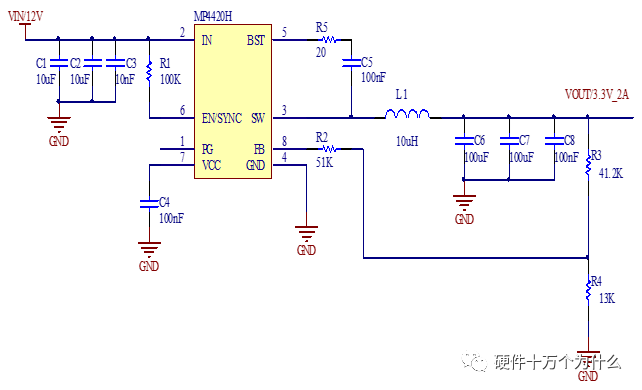
 If the signal frequency, there are:
 , expressed in decibels as:
  , it means that the signal can pass through the filter without attenuation;
  Time,
Time,  , expressed in decibels as:
 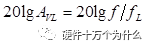 It means that the signal in this frequency band is attenuated by the slope of -20 dB/decade after passing through the filter;
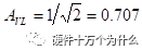 The signal attenuation is about 0.707 times.
  When Vo=0.99Vi, the test error is 1%.
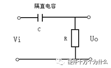
DC blocking capacitance (uF) 50W cutoff frequency (KHz) 50W-1% error frequency (KHz) 50W cutoff frequency (Hz) 1MW-1% error frequency (Hz) 0.1 31.83 222.82 1.5915 11.14 0.47 6.77 47.41 0.3386 2.37 1 3.18 22.28 0.1592 1.11 2.2 1.45 10.13 0.0723 0.51 10 0.32 2.23 0.0159 0.11 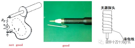


☞12ml Eliquid Capacity
☞600mAh Battery
☞Type-C Rechargeable
☞30mg/ml Nicotine Strength
☞6000 Puffs
-The firstpen -like prefilled pod starter kit you ever have
-Mesh coil for the pure and original taste
- Easy to tell the battery yolume by 7-color of LED indicators.
-12ml prefilled pods replaceable
-Type-Gcharging port design.
- Multiple colors, intense flavor and various experience
Cola Beats
Greer Gape
Peach lce
Margo ce
Kunquat Passion Fruit
Watermelon Ice
Cooll Mint
Lychee lce
Blueberry Raspberry
Strawberry lce Cream
Strawberry Ice
Mung Bean
