Various standard interface introductions and differences
Finding a particular embedded processor based on the application's performance, power, memory, and interface requirements is a daunting task for designers, because even similar systems have significant differences. Although the ARM? processor offers more than a dozen options, it is difficult for system designers to find a "perfect match."
This article will focus on the various standard interfaces and reveal the differences between them for different embedded chip vendors. Understanding the basic interface helps designers prioritize which interfaces should be on-chip. In addition, although standard interfaces are highly useful, in order to provide additional on-chip resources, a customizable on-chip interface is also required. This article describes two such peripheral blocks.
USBThe Universal Serial Bus (USB) interface was originally developed to connect personal computers and peripherals. Over time, it has become a common interface for industrial and infrastructure applications. Human Interface Devices (HIDs) such as keyboards, mice, and oscilloscopes typically use a USB interface, which means it must be supported by the system's embedded processor. The most effective way to achieve this is to use on-chip peripherals.
In addition to HID, two other devices are used for industrial and infrastructure applications. The USB Communication Device Class (CDC) is not only suitable for modems and fax machines, but also supports simple networking by providing an interface for Ethernet packet transmission. Similarly, USB mass storage devices (MSDs) are primarily used for hard drives and other storage media.
The USB 2.0 specification requires the host to initiate all inbound and outbound transfers. In addition, the specification defines three basic devices: host controllers, hubs, and peripherals.
The physical interconnection of USB 2.0 is a hierarchical star topology that uses a hub in each star center. Each line segment is a point-to-point connection between a host and a hub or function, or a hub connected to another hub or function.
The addressing scheme for devices in a USB 2.0 system enables up to 127 devices to be connected on a single host. These 127 devices can be any combination of hubs or peripherals. A composite or combined device can be two or more of these 127 devices.
While USB 2.0 is likely to be the first choice for industrial and many infrastructure applications, peripheral devices need to deploy Mobile USB (USB OTG) when communicating with each other without host involvement. To enable peer-to-peer communication, USB OTG introduces a new device that includes restricted host functionality for data sharing between two peripherals.
The OTG supplement defines a new set of handshaking methods called Host Negotiation Protocol (HNP). With HNP, a device that can be connected as a default peripheral can request to become a host. This helps the existing USB 2.0 host device paradigm to provide peer-to-peer communication. A Session Request Protocol (SRP) is also defined.
USB has the popularity and high status of a reliable standard, providing embedded processor manufacturers with a software library dedicated to USB functions, which can significantly reduce development time. System designers don't have to write their own code, they only need to make function calls to implement the interface.
These libraries should be certified to pass USB devices and embedded host compliance testing implemented by the USB Implementers Forum. Some vendors, such as Texas Instruments, offer a wide range of USB libraries for their embedded processors.
In 2007, the USB 3.0 Promoter Group was created to create a faster USB type that is backward compatible with previous USB standards and offers faster than USB 2.0 10 times the data rate. USB 3.0 uses a new signaling scheme and provides backwards compatibility by preserving the USB 2.0 2-wire interface. However, this faster version is still in the early stages of deployment, and USB 2.0 will remain the most popular USB type in the next few years, with high speed (480Mbps), low speed (1.5Mbps) and full speed (12Mbps) speed options.
EMACAlthough the interface conforming to the IEEE 802.3 Ethernet standard is generally mistakenly called the Ethernet Media Access Controller (EMAC), the complete EMAC subsystem interface actually includes three modules, which may be integrated on the chip. May not:
1. Physical layer interface (PHY);
2. Ethernet MAC, which can implement the EMAC layer of the protocol;
3. The custom interface is generally referred to as the MAC Control Module.
The EMAC module controls the packet data flow from the system to the PHY. The MDIO module performs PHY configuration and status monitoring. Both modules have access to the system core through the MAC Control Module, which also optimizes the data flow. In fully integrated solutions such as TI's embedded processors, custom interfaces are considered an integral part of EMAC/MDIO peripherals.
The complete EMAC subsystem is shown in Figure 1.
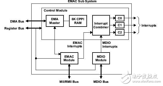
Figure 1: EMAC subsystem
The EMAC Control Module not only controls device interrupts, but also integrates an 8K byte internal random access memory (RAM) to hold the EMAC buffer descriptor. The MDIO module uses the 802.3 serial management interface to interrogate and control up to 32 Ethernet PHYs connected to the device using a shared two-wire bus.
The host software uses the MDIO module to configure auto-negotiation parameters for each PHY connected to the EMAC, restore the negotiation results, and configure the required parameters in the EMAC module for proper operation. This module provides near-transparent operation for the MDIO interface and requires little maintenance of the core processor.
The EMAC module provides an efficient interface between the network and the processor. The EMAC module typically provides 10Base-T (10Mbit/s) and 100Base TX (100Mbit/s), half-duplex and full-duplex modes, as well as hardware flow control and quality of service (QoS) support. In addition, some processors now support Gigabit EMAC capacity for 1000 Mbit/sec data rates.
Due to the widespread use of Ethernet, embedded processors typically integrate one or more EMAC interfaces on the chip. The methods used by different vendors to implement the above-described complete EMAC subsystem are also slightly different. The quality and scope of software support and libraries required to implement an Ethernet interface is another issue to consider when choosing an embedded processor vendor.
Sometimes there are more than one EMAC required for applications such as routers or switches. By using multiple EMACs, these applications can communicate with a wide range of devices while creating a synchronous process communication.
SATASerial ATA (SATA) connects a host bus adapter to a mass storage device such as a hard drive and an optical drive. It has basically replaced the previous Parallel ATA (PATA). PATA requires a 40/80 line parallel cable that is no longer than 18 inches in length. PATA's maximum data transfer rate is 133 Mbit/s, while the SATA serial data format uses two differential pairs to support the interface to the data storage device at line rates of 1.5 Gbit/s (SATA version 1) and 3.0 Gbit/s ( SATA version 2) with 6.0Gbit/s (SATA version 3). SATA 1 and SATA 2 are available now, and SATA 3 will be available soon.
In addition, SATA controllers require thinner cables and can be up to 3 feet long. Thinner cables are more flexible, allowing for easier wiring on the one hand and air circulation in the housing of large-capacity storage devices on the other.
Part of the reason for the high performance of serial links is the use of advanced system memory structures to accommodate high-speed serial data. This Advanced Host Controller Interface (AHCI) memory structure provides a common domain for control, status, and command list data tables. Each record in the command list contains information for programming the SATA device and a pointer to transfer data between the system memory and the device, pointing to the descriptor table.
Most SATA controllers not only support hot swap, but also use port multiplexers to increase the number of devices that can be connected to a single HBA port. The SATA standard has a long list of features, but few SATA controllers support all of these features. Common features include:
· Support for the AHCI Controller Specification version 1.1;
· Integrated SERDES PHY;
· Integrated Rx and Tx data buffers;
· Support SATA power management features;
· Each port is equipped with an internal DMA engine;
· Hardware-assisted native command sequencing (NCQ) for up to 32 records;
· 32-bit addressing;
· Support port multipliers;
· Support LED work;
· Mechanical presence switch.
Because SATA can store large amounts of data that can be extended to the terabyte range, it is widely used, including netbooks, laptops, desktops, multimedia devices, and portable data terminals. In addition, SATA can be used in industrial applications where sensors or system monitors may be required to store large amounts of data for later analysis.
DDR2/mobile DDRDDR2 is the successor to the Double Data Rate (DDR) SDRAM specification, which is not compatible with each other. DDR2 transfers data on the rising and falling edges of the bus clock signal and can run at higher bus speeds, enabling four transfers of data per internal clock cycle.
The simplified DDR2 controller includes the following design blocks:
· memory control;
· read interface;
· Write interface;
· and IO blocks.
These blocks and their relationship to the DDR2 memory chip and core logic are shown in Figure 2.
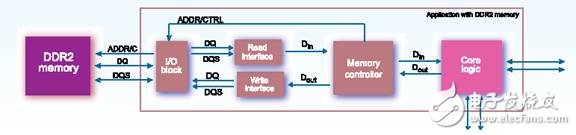
Figure 2: Implementation of a simplified DDR2 controller
The memory control block issues memory access to the dedicated core logic, and vice versa. The read physical block is responsible for processing the external signal timing of the data acquired during each read cycle, while the write physical block manages the clock and data issuance using the appropriate external signal timing.
Byte-wide bidirectional data strobe (DQS) is transmitted externally with data (DQ) for acquisition purposes. DQS is transmitted by the controller in edge-aligned mode when reading the memory, and center-aligned when writing to the memory. An on-chip delay phase-locked loop (DLL) is used to lock the DQS and the corresponding DQ. This ensures that they can track each other as the voltage and temperature change.
The DDR2 SRAM features a differential clock input that reduces the effects of clock input duty cycle variations. In addition, DDR2 SRAM supports data mask signals that add masks to data bits during each write cycle.
Mobile DDR (MDDR), also known as Low Power Double Data Rate Memory (LPDDR), operates at 1.8 V, while traditional memory operates at 2.5 V or 3.3 V and is commonly used in portable electronics. In addition, mobile DDR memory supports low power states not found in traditional DDR2 memories. As with all DDR memories, the double data transfer rate is achieved by simultaneously transferring data through the top and bottom of the device clock.
uPPSince the number of on-chip peripherals is constrained by cost or other constraints, system designers often want to find new ways to slice on-chip and off-chip. One strategy is to utilize resources that are not using video ports, and actually use it to send and receive non-video data at high speed. One of the drawbacks of this approach is that the data must be formatted into video frames, which requires some processor MIPS support in the work, and valuable programming time in the design cycle.
Other methods have similar difficulties, and most standard on-chip data interfaces are serial ports that cannot perform high-speed data transfers.
In the end, many system designers realized that a highly flexible, high-speed peripheral that could not be configured to meet specific interface standards but could be configured in multiple ways would be a significant advantage for data transmission. This idea is valuable if the system processor must be connected to a high-speed DAC, ADC, DSP, or FPGA to achieve high-speed data transfer of 250MB/sec.
The basic architecture of this peripheral is easy to describe. It has multiple channels with separate parallel buses that can be configured to accommodate more than one word in length. In addition, it also has an internal DMA block so that it does not have to take up the kernel's MIPS budget. Single and double data rates as well as multiple data packing formats are also available.
TI's various embedded processors offer Universal Parallel Port (uPP), including the Sitara® ARM9 AM1808 and AM1806 microprocessors (MPUs) and the OMAP-L138 processor with integrated TMS320C674x core and ARM9 core. Unlike serial peripherals such as SPI and UART, uPP offers designers the advantages of a parallel data bus with 8 bits and 16 bits per channel.
When running at the highest clock rate of 75MHz, uPP can transfer data at speeds far beyond the serial port peripherals. For example, a single 16-bit uPP channel running at 75MHz can be up to 24 times faster than an SPI peripheral running at 50MHz.
A simplified block diagram is shown in Figure 3.
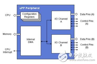
Figure 3: Simplified block diagram of uPP
The most important features of uPP include:
· Two independent channels with separate data buses;
o Both channels can operate in the same or opposite directions at the same time
· I/O speed is up to 75MHz, and the data bit width per channel is 8 ~ 16 bits;
· Internal DMA - can release CPU EDMA;
· Simple protocol with few control pins (configurable: 2 ~ 4 per channel);
· Single and double data rates (using single or double edges of the clock signal);
o Double data rate requires a maximum clock rate of 37.5MHz;
· Support multiple data packing formats with 9 ~ 15 bit data width;
· Data interleaving mode (limited to single channel).
uPP has some similarities to another TI peripheral-host port interface (HPI) that is dedicated to configurable data processing. HPI is a parallel interface that helps external hosts directly access the processor's internal memory. Unlike HPI, however, uPP does not allow external devices to access memory directly, it requires device software to queue I/O transfers. The biggest difference may be that uPP is much faster than HPI and the protocol is much simpler.
uPP is mainly used for applications such as FPGAs or DSPs that require off-chip real-time processing, and can bring great advantages to the market that requires real-time data such as medical fields. By using uPP, the decision processor can draw conclusions with the latest information.
PRUThe Programmable Real-Time Unit (PRU) is a small 32-bit processing engine that provides more resources for on-chip real-time processing. Designed specifically for TI's embedded processors in the AM1x MPU and OMPAP-L138 solutions, PRUs provide system designers with additional flexibility to reduce component costs.
The PRU's four-bus architecture facilitates the simultaneous transfer and execution of instructions with data transfers. In addition, an input register can be provided to allow external status information to be reflected in the status register of the internal processor.
An important goal of PRU design is to create as much flexibility as possible to perform various functions. The flexibility of the PRU helps developers integrate more interfaces into their end products, whether touch screens, integrated displays or storage functions, to further extend product functionality or their own proprietary interface capabilities. This goal is primarily achieved by providing full system visibility of PRUs including all system memory, I/O, and interrupts.
Although the PRU has full access to system resources, its internal resources are relatively common. It has 4K bytes of instruction memory and 512 bytes of data memory. In addition, the PRU has its own GPIO with a latency of only a few nanoseconds.
PRUs can implement custom logic by programming with simple assembly language code. The instruction set can be divided into four categories:
· Move data in or out of the processor's internal registers;
· Perform arithmetic operations;
· Perform logical operations;
· Control program flow.
In industrial applications, the PRU is typically configured as an IO block to replace the IO that the processor failed to provide. For example, it can be used in portable data terminals that require a combination of UART blocks to connect to GSM, GPS and Bluetooth, keypads, printers, LED groups, and RS232 ports. However, while the best option in this family of processors integrates only three UARTs, the PRU offers more UART interfaces to meet the needs of evolving end devices for handling a wide range of functions.
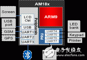
Figure 4: Extending the capabilities of existing device peripherals with PRUs
In addition to being used to replace IO, the PRU can be programmed to perform various controls, monitors, or other functions not provided on-chip. This flexibility is especially helpful for applications that contain control requirements that do not match the control requirements provided by any standard processor configuration.
ARM subsystem and peripheral integrationWhen evaluating peripheral interfaces in an ARM processor, it is important to understand how the peripherals are integrated with the ARM subsystem.
The ARM processor is suitable for complex, multitasking, general purpose control tasks. It not only provides memory for large programs, but also has good environment switching capabilities for running real-time operating systems (RTOS) and sophisticated advanced operating systems. ARM is responsible for system configuration and control, and its tasks include peripheral configuration and control, clock control, memory initialization, interrupt handling, and power management. The ARM subsystem contains the ARM processor and other components necessary to operate as the master controller of the overall processor system.
A typical ARM subsystem consists of the following component combinations:
· ARM core (eg ARM926EJ-S or ARM Cortex-A8?)
o Coprocessor 15 (CP15)
o MMU
o Write buffer
o instruction cache
o Data Cache
o Java accelerator
o Neon single instruction, multiple data (SIMD) coprocessor
o Vector Floating Point Coprocessor (VFP)
· ARM internal memory
o RAM
o ROM (ARM boot loader)
· Bus arbitrator
o Bus arbiter for accessing internal memory
o Bus arbiter for accessing system and peripheral control registers
o Bus arbiter for accessing external memory
· Debug, trace, and emulation modules
o JTAG
o ICECrusher?
o Embedded Trace Macro Unit (ETM)
· System control peripherals
o ARM interrupt control module
o Phase-locked loop (PLL) and clock control module
o Power management module
o System Control Module
See Figure 5 for a block diagram of a typical ARM9 ARM subsystem.
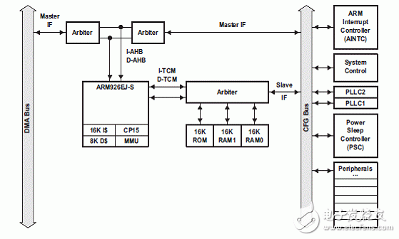
Figure 5: Block diagram of the ARM subsystem
For peripherals such as USB, EMAC, SATA, uPP, and PRU, the ARM subsystem has access to peripheral control and configuration registers, clocks, and power management controls.
in conclusionWhile standard interfaces play an important role in the system design process, interoperability and low cost can be achieved for designs, and the time required for design can be reduced, but for design teams that need to differentiate their products, their usefulness Still very limited. Designers should also rely on chip vendors to provide a variety of multi-component standard interfaces. For chip vendors, high-quality software libraries that help efficiently implement interfaces are other factors that enable differentiation. Providing a higher level of flexibility is also very helpful and can be obtained through configurable interfaces such as TI PRU and uPP. System designers use these options in their tool suite to be creative while keeping components low-cost.
Uv Air Purifier,Air Purifier With Uv Light,Uvc Air Purifier,Uv Air Cleaner
CIXI KYFEN ELECTRONICS CO.,LTD, , https://www.kyfengroup.com