AM demodulation circuit
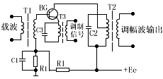
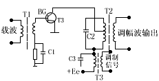
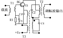
1. AM circuit The amplitude modulation circuit is to add the modulation signal and the carrier signal to a non-linear element (such as a crystal diode or triode) into a new frequency component through nonlinear transformation, and then use the resonant circuit to select the desired frequency component. The amplitude modulation circuit is divided into diode amplitude modulation circuit and transistor base amplitude modulation, emitter amplitude modulation and collector amplitude modulation circuit. Generally, triode amplitude modulation circuits are used. If the tuned amplifier uses low-power small-signal tuning amplifiers, it is called low-level amplitude modulation; otherwise, if it uses high-power large-signal tuning amplifiers, it is called high-level amplitude modulation. In practice, high-level amplitude modulation is mostly used, and its requirements are: (1) The modulation characteristics (the relationship between the modulation voltage and the output amplitude) are required to have good linearity; (2) The collector efficiency is high; (3) The requirements are low The amplifier circuit is simple. 1. Base amplitude modulation circuit Figure 1 is a transistor base amplitude modulation circuit. The carrier signal is added to the base of BG through a high-frequency transformer T1. The low-frequency modulation signal is connected in series with a high-frequency carrier through an inductive coil L. C2 is a high-frequency bypass capacitor and C1 is a low-frequency side. Circuit capacitor, R1 and R2 are biased voltage dividers. Due to the nonlinear effect of the ic = f (ube) relationship curve of the transistor, the collector current ic contains various harmonic components. Selected, the advantage of the base amplitude modulation circuit is that the low-frequency modulation signal power is small, so the low-frequency amplifier is relatively simple. The disadvantage is that it works in an under-voltage state, the collector efficiency is low, and the energy of the DC power supply cannot be fully utilized. 2. Emitter amplitude modulation circuit Figure 2 is the emitter amplitude modulation circuit, the principle is similar to the base amplitude modulation, because the voltage applied between the base and the emitter is about 1 volt, and the collector power supply voltage is more than ten volts to tens of volts, the modulation voltage is The influence of the collector circuit is negligible, so the working principle and characteristics of emitter amplitude modulation and base amplitude modulation are similar. 3. Collector amplitude modulation circuit Figure 3 is a collector amplitude modulation circuit. The low-frequency modulation signal is introduced from the collector. Because it operates in an overvoltage state, the efficiency is higher but the nonlinear distortion of the modulation characteristic is more serious. In order to improve the modulation characteristic, a non-linear signal can be introduced in the circuit. Linear compensation measures to make the input excitation voltage change with the collector power supply voltage. For example, when the collector power supply voltage decreases, the excitation voltage amplitude will decrease accordingly, and will not enter a strong voltage state; conversely, when the collector power supply voltage increases , It will increase accordingly, and will not enter the undervoltage region. Therefore, the amplitude modulator always works in a weak overvoltage or critical state, which can not only improve the modulation characteristics, but also have higher efficiency. The circuit to achieve this measure is called Double collector amplitude modulation circuit. Using the dual amplitude modulation circuit of the collector and emitter of FIG. 4 can also improve the modulation characteristics. Note that the same-named end of the transformer, while the positive half-wave of the modulation signal, although the collector supply voltage increases, at the same time the base bias voltage also becomes positive, which prevents the undervoltage operation state; when the negative half-wave of the modulation signal Although the collector voltage decreases, the base extreme bias voltage also becomes negative, so that it does not enter the strong overvoltage region, and thus keeps working in a critical and weak overvoltage state. Figure 1. Base-amplitude modulation circuit Figure 2. Emitter-amplitude modulation circuit Figure 3. Collector amplitude modulation circuit Figure 4. Double amplitude modulation circuit Second, the amplitude detection circuit The process of taking out the modulated signal from the amplitude-modulated wave is called amplitude detection. There are three common detection circuits: small-signal square-law detection, large-signal envelope full-wave detection, and product detection. (1) Detection efficiency (voltage transmission coefficient) If the peak value of the detector input constant amplitude high-frequency voltage is Uc, and the output voltage after detection is Uo, the detection efficiency K is defined as: K = Uo / Uc If the input of the detector is an envelope amplitude modulation wave, the detection efficiency is defined as the ratio of the output low frequency voltage amplitude UΩ to the input high frequency voltage envelope amplitude mUc: K = UΩ / mUc In the formula: m is the amplitude modulation coefficient. The larger K indicates that a larger low-frequency output signal can be obtained under the same input condition, that is, the detection efficiency is high. (2) Detection distortion It reflects the conformity of the output low-frequency voltage waveform and the input modulated wave including shape. (3) Input resistance Ri The equivalent resistance seen by the input end of the detector is called the input resistance Rio. Usually the detector is connected to the output end of the intermediate frequency amplifier, and Ri is regarded as its load. Therefore, the greater the Ri, the smaller the impact on the IF amplifier, 1. Small signal square law detector Figure 5 (a) is a small signal detection circuit. Its characteristics are: (1) The amplitude of the input high-frequency signal ui (t) is on the order of tens of millivolts; (2) Select the appropriate bias voltage so that the operating point Q is on the curved section of the volt-ampere characteristic [see Figure 5 (b)], current flows through the diode during the entire high-frequency signal period. Through theoretical analysis, the output voltage u2 and input voltage U of the detector (1) Detection efficiency K = UΩ / mUc = Ra2Uc / (1 + a1R [Response of test question output voltage] In the formula: R is the load resistance of the detector, Uc is the carrier amplitude of the high-frequency amplitude modulation wave, a1 and a2 are the coefficients related to the operating point current, and its value is approximately: a1 = 38Io and a2 = 0.74 × 10 If the working point current of the detector is selected as Io = 20 μA, R = 4.7 kOhm, Uc = 50 mV, the detection efficiency is: K = Ra2Uc / (1 + a1R) = (4.7 × 10 (2) Non-linear distortion. Since the second harmonic is very close to the fundamental wave, it is not easy to clear it. Therefore, the second harmonic distortion coefficient y is often used to estimate the size of the distortion. Its value is: y = m / 4 It can be seen from the formula that the greater the amplitude modulation coefficient m, the greater the y, and the more severe the distortion. In general, m≈30%, then y≈7.5% (3) Input impedance Ri, AC impedance with exponential wave frequency ωc. It can be seen from Figure 5 (a) that for ωc, C is regarded as a short circuit, so Ri is equal to the AC resistance rd of the diode, and its value at room temperature is: Ri = rd = 26 × 10 If Io = 20 uA, then Ri = (26 × 10 The shortcomings of small signal detection are: low input impedance, serious nonlinear distortion, 2. Daxin Diao Peak Envelope Detection As shown in Figure 6 (a), it is a large-signal detection circuit. Because the AC part of the output voltage is proportional to the maximum value of the modulation signal, it is also called linear detection. Its characteristics are: (1) The input voltage amplitude is generally more than 500 mV; ( 2) There is no bias voltage E, due to the reverse effect of the output voltage, the operating point is actually in the section where u <0 [see Figure 6 (b)]. Therefore, the large-signal detection diode only finds out for a period of time within one week of the carrier wave, and ends at another period of time. The main parameters of the large signal peak diode detector are calculated as follows: K = cosθ Table I Relation table of rd / R, Ri / R and θ rd / R 0 0.00057 0.0046 0.017 0.045 0.1 0.22 0.51 1.36 OO θ 0 ° 10 ° 20 ° 30 ° 40 ° 50 ° 60 ° 70 ° 80 ° 90 ° cosθ 1 0.99 0.94 0.87 0.77 0.64 0.50 0.34 0.17 0 Ri / R 0.50 0.51 0.54 0.59 0.69 0.84 0.11 0.69 3.5 OO Where: θ is the semi-conducting angle, which depends on the rd / R value, the relationship between the two is rd / R = (tgθ-θ) / π According to the rd / R value, the K value can be directly found through Table 1 (2) Input impedance Ri Ri / R = (tgθ-θ) / (θ-sinθcosθ) It can be seen that the input impedance Ri is determined by the angle θ, which is determined by the rd / R value. Therefore, the input impedance Rio can be directly found through Table 1 according to the rd / R value (3) Detection distortion There are often two types of distortion: one is diagonal cutting distortion, and the other is bottom cutting distortion. Figure 7 shows the diagonal cutting distortion. The reason for this distortion is that the filter time constant RC is too large, so that the discharge rate of the filter capacitor cannot keep up with the envelope change rate. To prevent diagonal cutting distortion, The time constant RC should satisfy the following relationship: RC <( Another kind of cutting distortion is caused by the difference between the low-frequency AC load of the detector and the resistance of the DC load. Usually the low-frequency voltage output by the detector is sent to the low-frequency amplifier through the coupling circuit [R1C1 in Figure 7 (a)]. Because of C1 The value is very large, (about 10 microfarads) the DC voltage drop across its two ends is the average value of the carrier amplitude Uco if R1 m In the formula: R is DC resistance, AC resistance R- = R // R1. The undistorted condition can be written as m Figure 8 (b) is the filter circuit of the TV receiver. Since the modulated signal is an image signal up to 6 MHz, in order to prevent diagonal cutting distortion, the capacitor C1 only selects 10 picofarads, but it is not enough to filter the carrier wave by itself. It also needs to be connected to the LC2 filter. The diode is connected in series with a small resistance of 200 ohms to increase the signal and compensate for the reduction of the internal resistance of the diode, so that the transmission coefficient is relatively stable. In fact, the detection linearity is also improved. Figure 8 Radio and TV detection circuit
·Basic precautions
Do not put expensive oil into low-quality cartridges to avoid wastage. Most pre-filled oil cartridges have the so-called 510 thread. The oil cartridge screws onto a rechargeable battery. Some of these batteries have buttons and some heat up automatically when you pump the oil. Some batteries have multiple temperature settings and some heat up to a preset temperature; these features need to be known in advance.
·Cleaning notes
Use a suitable cleaning tool to clean them, such as activated charcoal or dried tea leaves in a used pipe to absorb the oil. It is important not to use alcohol or other boiling water to clean the pipe, and to wait until it has cooled down completely before cleaning. Otherwise, the hot stem will come into contact with the watery liquid and cause the mouthpiece tenon to loosen, thus shortening the life of the 510 cartridges.
This is what you should be aware of when using 510 cartridges. At the same time, when using 510 cartridges, there are still some vaping tips, for example, when using them, be careful not to suck too hard, will not produce smoke. When you inhale too hard, the smoke is sucked directly into your mouth and not atomized by the atomizer, so gently inhaling is more powerful and gives you a better vaping experience.
510 Cartridge Oem,Leakproof 510 Cartridge,510 Battery And Cartridges Oem,510 Cartridge Shenzhen MASON VAP Technology Co., Ltd. , https://www.e-cigarettefactory.com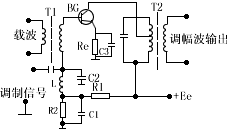
 c is proportional to the square law detection is named after it, its parameters are as follows:
  Io (the unit of Io is ampere)
  × 0.47 × 10
  × 20 × 10
  × 50 × 10
  ) / (1 + 38 × 20 × 10
  × 4.7 × 10
  ) = 0.76
  / Io
/ Io  ) / 20 × 10
  = 1.3 thousand ohms
 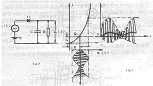 Figure 5
 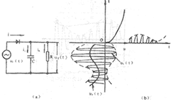 Image 6
  / m) × (TΩ / 2π) where: m is the amplitude modulation coefficient, TΩ = 2π / Ω, if m = 0.3, then RC <0.5TΩ
 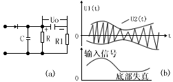 Picture 7