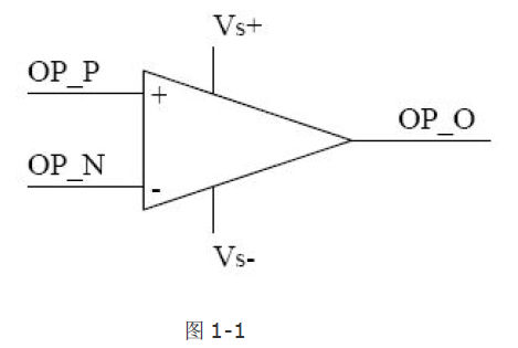
How to form a basic operational amplifier circuit
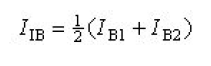
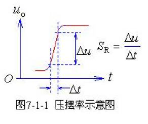
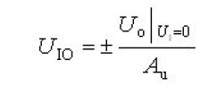
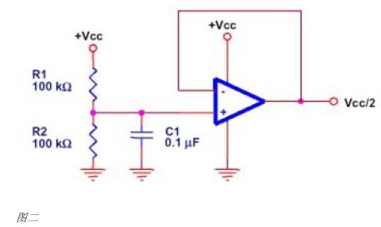
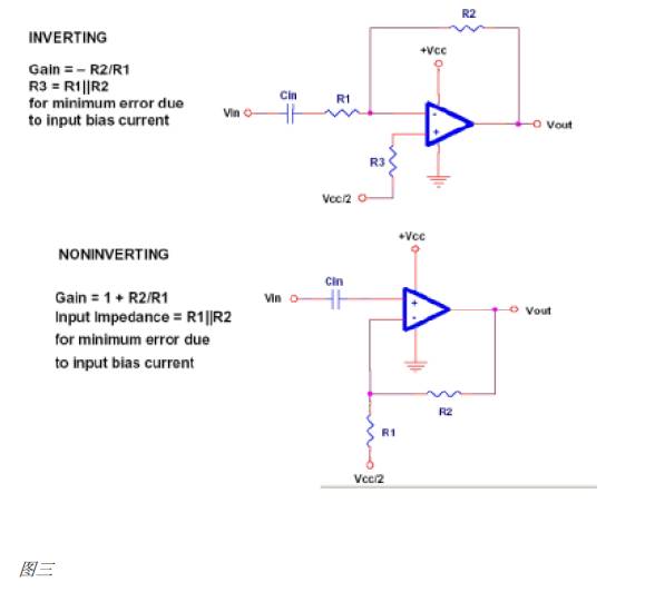
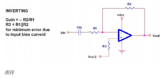
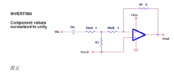
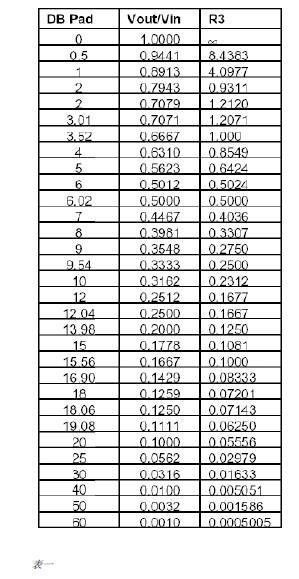
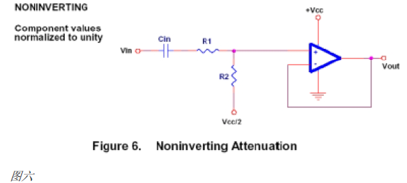
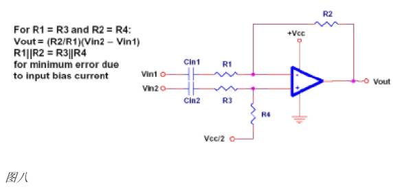
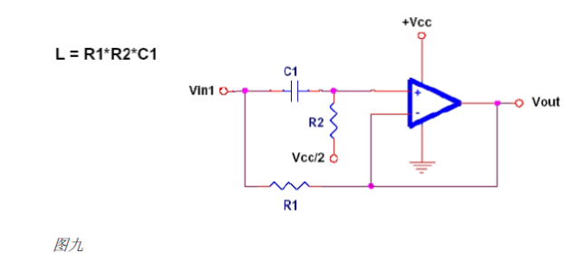
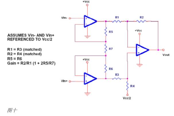
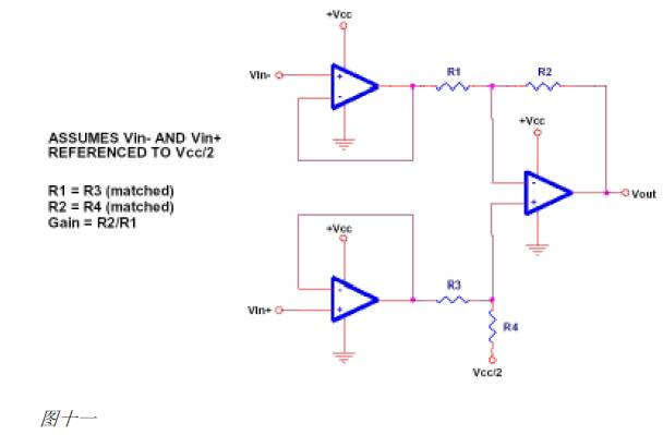
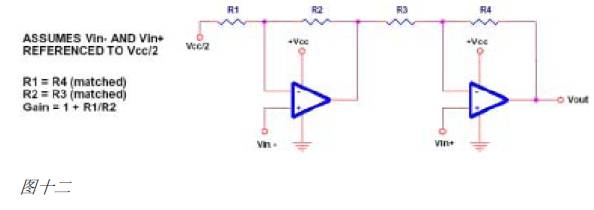
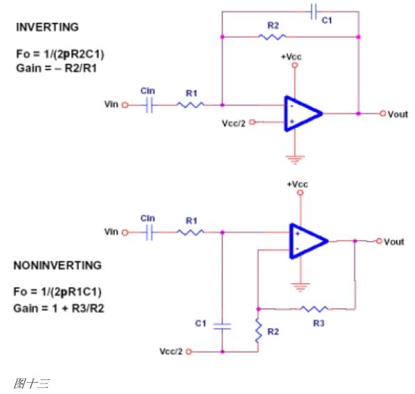
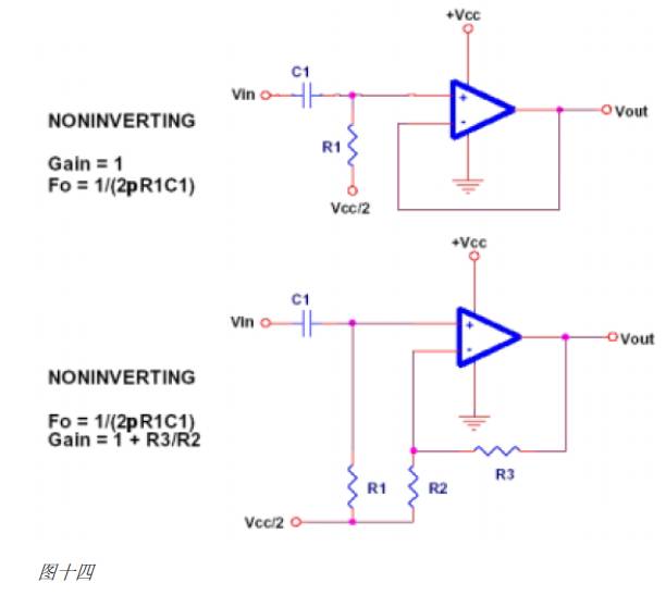
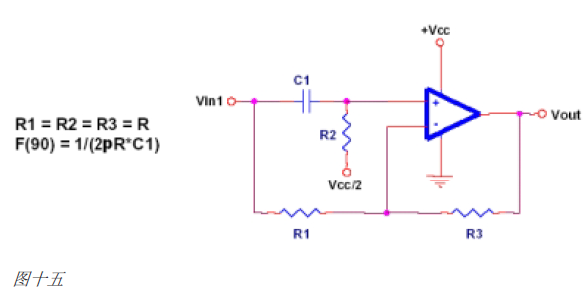
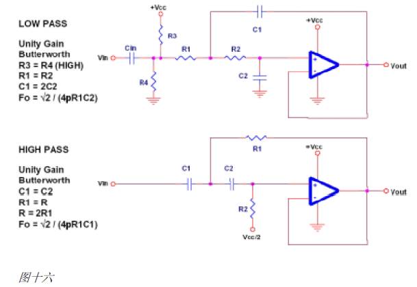
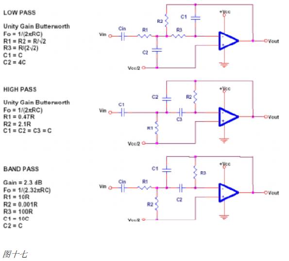
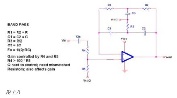
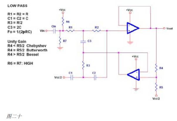
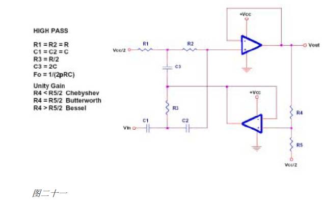
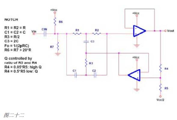
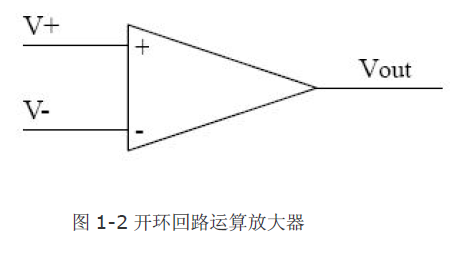
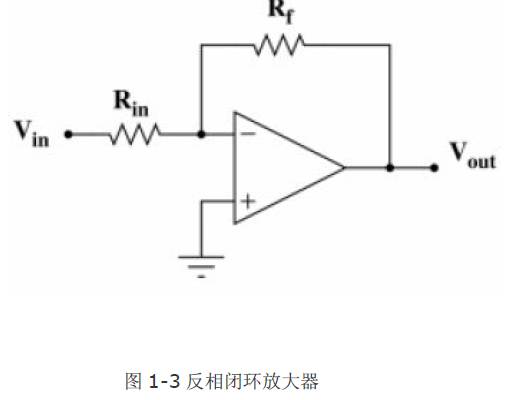
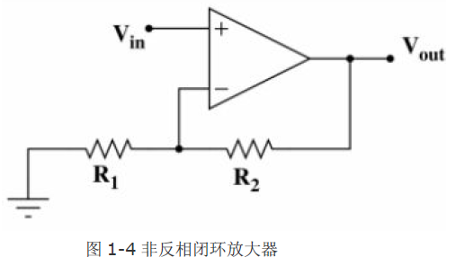
Introduction We often see a lot of very classic operational amplifier application atlases, but these applications are built on the basis of dual power supplies. In many cases, circuit designers must use a single power supply, but they don’t know how to use dual power supplies. The circuit is converted into a single power supply circuit. When designing a single-supply circuit, you need to be more careful than a dual-supply circuit, and the designer must fully understand the content described in this article. 1.1 Power supply and single power supply All operational amplifiers have two power supply pins. Generally, in the data, their logos are VCC+ and VCC-, but sometimes their logos are VCC+ and GND. This is because the authors of some data sheets attempt to use this identification difference as the difference between a single-supply op amp and a dual-supply op amp. However, this does not mean that they have to be used that way-they may be able to work at other voltages. When the op amp is not powered by the default voltage, you need to refer to the data sheet of the op amp, especially the absolute maximum supply voltage and voltage swing instructions. Most analog circuit designers know how to use operational amplifiers under dual power supply voltage conditions. For example, the circuit on the left in Figure 1. A dual power supply is composed of a positive power supply and a negative power supply of equal voltage. Generally, plus or minus 15V, plus or minus 12V and plus and minus 5V are also frequently used. Both the input voltage and the output voltage are given with reference to the ground, including the swing amplitude limit Vom of the positive and negative voltages and the maximum output swing. The single power supply circuit (right in Figure 1) has the power pin of the op amp connected to the positive power supply and ground. The positive power supply pin is connected to VCC+, and the ground or VCC- pin is connected to GND. The voltage obtained by dividing the positive voltage into half is connected to the input pin of the op amp as a virtual ground. At this time, the output voltage of the op amp is also the virtual ground voltage. The output voltage of the op amp is centered on the virtual ground and swings between Vom. Inside. There are some new op amps with two different maximum and minimum output voltages. The data sheet of this kind of op amp will specify Voh and Vol separately. It is important to note that many designers will use virtual ground to refer to the input voltage and output voltage at will. However, in most applications, the input and output are referenced to the power ground, so the designer must refer to the input and output Add a DC blocking capacitor to the place where it is used to isolate the DC voltage between the virtual ground and the ground. Usually the voltage of a single power supply is generally 5V, and the output voltage swing of the op amp will be lower at this time. In addition, the current supply voltage of the op amp can also be 3V or even lower. For this reason, the op amps used in circuits powered by a single power supply are basically Rail-To-Rail op amps, which eliminates the lost dynamic range. It should be pointed out that the input and output are not necessarily able to withstand the voltage of Rail-To-Rail. Although the device is specified as Rail-To-Rail, if the output or input of the op amp does not support rail-to-rail, a voltage close to the input or output voltage limit may degrade the function of the op amp, so it is necessary Carefully refer to the data sheet to see if the input and output are rail-to-rail. Only in this way can it be ensured that the function of the system will not be degraded, which is the obligation of the designer. 1.2 Virtual ground Single-supply operational op amps need an external virtual ground. Normally, this voltage is VCC/2. The circuit in Figure 2 can be used to generate VCC/2 voltage, but it will reduce the low-frequency characteristics of the system. R1 and R2 are of equal value and are selected by the allowable consumption and allowable noise of the power supply. The capacitor C1 is a low-pass filter used to reduce the noise from the power supply. In some applications, the buffered op amp can be ignored. In the following, the virtual ground of some circuits must be generated by two resistors, but this is not a perfect method. In these examples, the resistance value is greater than 100K. When this happens, it is noted in the circuit diagram. 1.3 The AC coupling virtual ground is the DC level greater than the power ground, which is a small, local ground level, which creates a potential problem: the input and output voltages are generally referenced to the power ground. If you directly connect the signal source The output is connected to the input of the op amp, which will produce unacceptable DC offset. If this happens, the op amp will not respond correctly to the input voltage, because this will cause the signal to exceed the allowable input or output range of the op amp. The solution to this problem is to use AC coupling between the signal source and the op amp. Using this method, both the input and output devices can refer to the system ground, and the op amp circuit can refer to the virtual ground. When more than one op amp is used, it is not necessary to use the coupling capacitor between the stages if the following conditions are met: the reference ground of the first stage op amp is the virtual ground, and the reference of the second stage op amp is also the virtual ground. Each stage of the op amp has no gain. Any DC bias will be multiplied by the gain in any stage and may cause the circuit to exceed its normal operating voltage range. If in any doubt, assemble a prototype with coupling capacitors, then remove one of them at a time and observe whether the electrical work is normal. Unless both the input and output are referenced to the virtual ground, there must be a coupling capacitor to isolate the signal source from the op amp input, as well as the op amp output and the load. A good solution is to disconnect the input and output, and then check the DC voltage on the two input pins of all op amps and the output pin of the op amp. All voltages must be very close to the virtual ground voltage. If not, the output of the previous stage must be isolated by a capacitor. (Or there is a problem with the circuit) 1.4 Combination op amp circuit In some applications, the combination op amp can be used to save cost and board space, but it will inevitably cause mutual coupling, which can affect filtering, DC bias, Noise and other circuit characteristics. Designers usually start designing from independent functional prototypes, such as amplification, DC bias, filtering, and so on. Unite them after verifying each unit module. Unless otherwise specified, the gain of all filter units in this article is 1. 1.5 Choosing the values ​​of resistors and capacitors Everyone who is just starting to do analog design wants to know how to choose component parameters. Should I use 1 ohm or 1 megohm for the resistor? Generally speaking, the resistance value in the K ohm level to 100K ohm level is more suitable for ordinary applications. In high-speed applications, the resistance is between 100 ohms and 1K ohms, but they will increase power consumption. In the portable design, the resistance is in the 1 mega-ohm to 10 mega-ohm class, but they will increase the noise of the system. The basic equations used to select the resistor and capacitor values ​​to adjust the circuit parameters have been given in each figure. If used as a filter, the accuracy of the resistance should be 1% E-96 series (refer to Appendix A). Once the magnitude of the resistance value is determined, select a standard E-12 series capacitor. E-24 series capacitors are used for parameter adjustment, but they should not be used as much as possible. The capacitor used for circuit parameter adjustment should not be 5%, but 1%. 2.1 There are two basic types of amplifying and amplifying circuits: non-inverting amplifiers and inverting amplifiers. Their AC coupled version is shown in Figure 3. For AC circuits, reverse means that the phase angle is shifted by 180 degrees. This circuit uses a coupling capacitor-Cin. Cin is used to prevent the circuit from generating DC amplification, so that the circuit will only amplify the AC. If Cin is omitted in the DC circuit, then the DC amplification must be calculated. In high frequency circuits, it is very important not to violate the bandwidth limit of the op amp. In practical applications, the gain of the first-stage amplifying circuit is usually 100 times (40dB), and a higher magnification will cause the circuit to oscillate, unless you pay attention to it when laying out the board. If you want to get a large amplifier with a comparative amplification factor, it is better to use two equal gain op amps or multiple equal gain op amps than one op amp. 2.2 Attenuation The traditional inverting attenuator composed of operational amplifiers is shown in Figure 4. R2 is smaller than R1 in the circuit. This method is not recommended, because many op amps are not suitable for working with magnifications less than 1x. The correct way is to use the circuit shown in Figure 5. A set of normalized R3 resistance values ​​in Table 1 can be used to generate different levels of attenuation. For resistance values ​​that are not in the table, you can use the following formula to calculate R3=(Vo/Vin)/(2-2(Vo/Vin)). If there are values ​​in the table, proceed as follows: Rf and Rin are between 1K and Choose a value between 100K and use this value as the base value. Divide Rin by two to get RinA and RinB. Multiply the basic value by 1 or 2 to get Rf, Rin1, and Rin2, as shown in Figure 5. Choose a suitable scale factor for R3 in the table, and then multiply it by the base value. For example, if Rf is 20K, and both RinA and RinB are 10K, then a 12.1K resistor can get -3dB attenuation. The in-phase attenuator in Figure 6 can be used as a voltage attenuation and in-phase buffer. 2.3 Adder Figure 7 is an inverting adder, which is a basic audio mixer. But this circuit is rarely used in real audio mixers. Because this will approach the operating limit of the op amp, we actually recommend increasing the power supply voltage to increase the dynamic range. In-phase adders are achievable, but they are not recommended. Because the impedance of the signal source will affect the gain of the circuit. 2.4 The subtractor is like an adder. Figure 8 is a subtractor. A common application is to remove the original vocal in a stereo tape and leave the accompanying sound (the original vocal level in the two channels is the same when recording, but the accompanying sound is slightly different). 2.5 Simulating the inductance The circuit in Figure 9 is a circuit that reverses the capacitance and is used to simulate the inductance. The inductance will resist the change of the current, so when a DC level is applied to the inductance, the rise of the current is a slow process, and the voltage drop on the resistance in the inductance is particularly important. 2.6 Instrument amplifier The instrument amplifier is used in the occasions that need to amplify the small-level signal DC signal, it is from the subtractor topology. The instrument amplifier takes advantage of the high impedance at the non-inverting input. The basic instrument amplifier is shown in Figure 10. The gain of this circuit is very easy to calculate. But this circuit also has a disadvantage: that is, the two resistors in the circuit must be replaced together, and they must be of equal value. Another disadvantage is that the first-stage op amp does not produce any useful gain. In addition, two operational amplifiers can also be used to form an instrument amplifier, as shown in Figure 12. However, this instrument amplifier is not recommended, because the amplification of the first op amp is less than one, so it may be unstable, and the signal on Vin- takes more time than the signal on Vin+ to arrive. The output terminal. This section gives a very in-depth introduction to active filters composed of op amps. In many cases, in order to block the DC level caused by the virtual ground, a capacitor is connected in series to the input terminal of the op amp. This capacitor is actually a high-pass filter. In a sense, a single-supply op amp circuit like this has such a capacitor. The designer must determine that the capacity of this capacitor must be more than 100 times larger than the capacity of other capacitors in the circuit. Only in this way can it be ensured that the amplitude-frequency characteristics of the circuit will not be affected by this input capacitance. If this filter also has an amplifying effect, the capacity of this capacitor is preferably more than 1000 times the capacity of other capacitors in the circuit. If the input signal already contains the DC bias of VCC/2, this capacitor can be omitted. The output of these circuits all include the DC bias of VCC/2. If the circuit is the last stage, then the output capacitor must be connected in series. There is an agreement about filter design. The filters here are composed of op amps powered by a single power supply. The implementation of the filter is very simple, but the designer must pay attention to the following points: 1. The inflection point (center) frequency of the filter 2. The gain of the filter circuit 3. The Q value of the band pass filter and the band stop filter 4. Types of low-pass and high-pass filters (Butterworth, Chebyshev, Bessell) Unfortunately, it is impossible to use an op amp to get a perfectly ideal filter. Even if possible, the designer must use very complicated calculations to complete the filter design due to the negative mutual inductance between the various components. Generally, the more complex the waveform control requirements, the more op amps are needed, which will be determined based on the maximum distortion that the designer can accept. Or it can be finalized through several experiments. If the designer wants to implement the filter with a minimum of components, then there is no choice but to use a traditional filter, which can be obtained by calculation. 3.1 First-order filters First-order filters are the simplest circuits. They have an amplitude-frequency characteristic of 20dB per octave. 3.1.1 Low-pass filters A typical low-pass filter is shown in Figure 13. 3.1.2 High-pass filter A typical high-pass filter is shown in Figure 14. 3.1.3 Wien filter The Wien filter has the same gain for all frequencies, but it can change the phase angle of the signal and is also used as a phase angle correction circuit. The circuit in Figure 15 has a 90-degree phase shift for a signal with a frequency of F, a zero-degree phase shift for DC, and a 180-degree phase shift for high-frequency signals. 3.2 Second-order filter Second-order filter circuits are generally named after their inventors. A few of them are still in use today. There are some second-order filter topologies that can form low-pass, high-pass, band-pass, and band-stop filters, but some do not. Not all filter topologies are listed here, but those that are easy to implement and easy to adjust are listed. The second-order filter has an amplitude-frequency characteristic of 40dB per octave. Usually bandpass and bandstop filters composed of the same topology use the same components to adjust their Q values, and they change the filter between Butterworth and Chebyshev filters. It must be known that only the Butterworth filter can accurately calculate the inflection point frequency, and the Chebyshev and Bessell filters can only be fine-tuned on the basis of the Butterworth filter. The bandpass and bandstop filters we usually use have very high Q values. If you need to implement a wide band pass or band stop filter, you need to connect a high pass filter and a low pass filter in series. The pass characteristic of the band pass filter will be the overlapping part of the two filters, and the pass characteristic of the band rejection filter will be the non-overlapping part of the two filters. Inverted Chebyshev and Elliptic filters are not introduced here, because they are no longer in the scope of the circuit set that needs to be introduced. Not all filters can produce the results we envisioned-for example, the attenuation amplitude of the filter at the end of the stopband will be greater in the multi-feedback filter than in the Sallen-Key filter. Because these characteristics are beyond the scope of the circuit atlas, please go to the textbook to find the advantages and disadvantages of each circuit. However, the circuit introduced here is used in not very special circumstances, and the results are acceptable. 3.2.1 Sallen-Key filter Sallen-Key filter is a popular and widely used second-order filter. His cost is very low, only one operational amplifier and four passive components are required. But changing to Butterworth or Chebyshev filters is not so easy to adjust. Please refer to the reference item [1] and reference item [2] for the designer, which introduces the details of various topologies. This circuit is a unity gain circuit. Changing the gain of the Sallen-Key filter also changes the amplitude-frequency characteristics and type of the filter. In fact, the Sallen-Key filter is a Butterworth filter with a gain of 1. 3.2.2 Multi-feedback filter The multi-feedback filter is a universal, low-cost and easy-to-implement filter. Unfortunately, the calculations at design time are a bit complicated, so I won’t go into the details here. Please refer to the detailed introduction of multiple feedback filters in the reference entry [1]. If what is needed is a unity gain Butterworth filter, then the circuit here can give an approximate result. 3.2.3 Double T filter The double T filter can be realized with one op amp or two op amps. It is based on a passive network composed of three resistors and three capacitors. The matching of these six components is critical, but fortunately this is still an easy process. This network can be composed of resistors of the same value and capacitors of the same value. Using the formula in the figure, R3 and C3 can be calculated at the same time. Should try to choose the same batch of components, they have very similar characteristics. 3.2.3.1 Realization of single op amp 3.2.3.2 Dual operational amplifiers to achieve typical dual operational amplifiers are shown in Figure 20 to Figure 22 Open loop Closed-loop negative feedback connects the reverse input and output of the operational amplifier, and the amplifier circuit is in a negative feedback configuration. At this time, the circuit can usually be simply called a closed-loop amplifier. The closed-loop amplifier enters the end point of the amplifier according to the input signal, and can be divided into two types: inverting amplifier and non-inverting amplifier. The inverting closed-loop amplifier is shown in Figure 1-3. Assuming that this closed-loop amplifier uses an ideal operational amplifier, because its open-loop gain is infinite, the two inputs of the operational amplifier are virtual ground, and the relationship between its output and input voltage is as follows: Vout=-(Rf/ Rin)*Vin Closed-loop positive feedback connects the positive input terminal and output terminal of the operational amplifier, and the amplifier circuit is in a positive feedback state. Since the positive feedback configuration works in an extremely unstable state, it is mostly used in applications that need to generate oscillating signals. in. Ideal op amp and ideal op amp conditions When analyzing and synthesizing an op amp application circuit, in most cases, the integrated op amp can be regarded as an ideal op amp. The ideal op amp, as the name suggests, is to idealize the various technical indicators of the integrated op amp. Since the technical indicators of the actual op amp are relatively close to the ideal op amp, the error caused by idealization is very small and can be ignored in general engineering calculations. The technical specifications of the ideal op amp are as follows: 1. The open-loop differential mode voltage amplification factor Aod=∞; 2. Input resistance Rid=∞; output resistance Rod=03. Input bias current IB1=IB2=0; 4. Offset voltage UIO, offset current IIO, offset voltage temperature drift From the point of view of use, the bias current is better, and the output voltage change caused by the change of the internal resistance of the signal source is also smaller, so the input bias current is an important technical indicator. Generally, IIB is about 1nA~0.1μA. Input offset voltage temperature drift △UIO/△T The input offset voltage temperature drift refers to the ratio of the input offset voltage change with temperature to the temperature change within the specified operating temperature range. It is an important indicator to measure the temperature drift of the circuit and cannot be compensated by an external zero-adjusting device. The smaller the input offset voltage temperature drift, the better. The input offset voltage temperature drift of a general operational amplifier is between ±1mV/℃~±20mV/℃. The input offset current temperature drift △IIO/△T is within the specified operating temperature range, and the ratio of the input offset current change with temperature to the temperature change is called the input offset current temperature drift. The input offset current temperature drift is a measure of the current drift of the amplifier circuit and cannot be compensated by an external zero adjustment device. High-quality op amps are several pA per degree. The maximum differential mode input voltage Uidmax The maximum differential mode input voltage Uidmax refers to the maximum differential mode input voltage that the two input terminals of the op amp can withstand. Above this voltage, the op amp input stage pair tube will enter the non-linear region, which will significantly deteriorate the performance of the op amp and even cause damage. Depending on the process, Uidmax is about ±5V~±30V. Maximum common-mode input voltage Uicmax The maximum common-mode input voltage Uicmax refers to the maximum common-mode input voltage that the op amp can withstand under the normal operating conditions of the op amp. When the common-mode voltage exceeds this value, the operating point of the input differential pair tube enters the nonlinear region, the amplifier loses the common-mode rejection capability, and the common-mode rejection ratio drops significantly. The maximum common-mode input voltage Uicmax is defined as the common-mode input voltage value that causes the output voltage to produce 1% following error when the op amp is connected as a voltage follower under the nominal power supply voltage; or it is defined as the common-mode applied when it drops by 6dB Enter the voltage value. The open-loop differential-mode voltage amplification factor Aud refers to the ratio of the change in output voltage to the change in the input voltage at the input port of the integrated op amp working in the linear region and connected to the specified load. The Aud of the operational amplifier is between 60 and 120 dB. Op amps with different functions are very different in Aud. The differential mode input resistance Rid refers to the input resistance of the op amp when the differential mode signal is input. The larger the Rid, the smaller the impact on the signal source. The input resistance Rid of the op amp is generally more than a few hundred kiloohms. The definition of op amp common-mode rejection ratio KCMR is the same as that in the differential amplifier circuit. It is the ratio of differential-mode voltage amplification to common-mode voltage amplification, usually expressed in decibels. Op amps with different functions have different KCMRs, some are between 60-70dB, and some are as high as 180dB. The larger the KCMR, the stronger the ability to suppress common mode interference. Open-loop bandwidth BW open-loop bandwidth, also known as -3dB bandwidth, refers to the frequency fH corresponding to the 3dB drop of the operational amplifier's differential mode voltage amplification factor Aud in the high frequency band. The unity gain bandwidth BWG refers to the frequency fT corresponding to when the signal frequency increases and the Aud drops to 1, that is, the signal frequency fT when the Aud is 0dB. It is an important parameter of integrated op amp. The fT of the 741 op amp is 7Hz, which is relatively low. Slew rate SR (slew rate) Open-loop bandwidth: The open-loop bandwidth is defined as inputting a small constant amplitude sinusoidal signal to the input terminal of the op amp, and the open-loop voltage gain measured from the output terminal of the op amp drops 3db from the DC gain of the op amp (or equivalent The signal frequency corresponding to 0.707 of the DC gain of the op amp. This is used for very small signal processing. Unity gain bandwidth GB: The unity gain bandwidth is defined as a constant amplitude sinusoidal small signal input to the input terminal of the op amp under the condition that the closed loop gain of the op amp is 1 times, and the closed loop voltage gain measured from the output end of the op amp drops 3db (Or equivalent to 0.707 of the input signal of the op amp) corresponding to the signal frequency. The unity gain bandwidth is a very important indicator. For small sinusoidal signal amplification, the unity gain bandwidth is equal to the product of the input signal frequency and the maximum gain at that frequency. In other words, when you know the signal frequency to be processed and the signal required After the increase, the unity gain bandwidth can be calculated to select the appropriate op amp. This is used for op amp selection in small signal processing. Slew rate (also known as slew rate) SR: The slew rate of the op amp is defined as the input of a large signal (including step signal) to the input of the op amp and the output of the op amp when the op amp is connected in a closed loop. The output rise rate of the op amp is measured at the end. Since the input stage of the op amp is in the switching state during the conversion, the feedback loop of the op amp does not work, that is, the conversion rate has nothing to do with the closed-loop gain. The slew rate is a very important indicator for large signal processing, and the slew rate is SR10V/μs for general operational amplifiers. The highest conversion rate SR of current high-speed operational amplifiers reaches 6000V/μs. This is used for op amp selection in large signal processing. Full power bandwidth BW: Full power bandwidth is defined as, when the closed-loop gain of the op amp is 1 times at the rated load, a constant amplitude sinusoidal signal is input to the input end of the op amp to maximize the output amplitude of the op amp (Allowing a certain amount of distortion) signal frequency. This frequency is limited by the conversion rate of the op amp. Approximately, the full power bandwidth = conversion rate / 2πVop (Vop is the peak output amplitude of the op amp). Full power bandwidth is a very important indicator, used for op amp selection in large signal processing. Settling time: The settling time is defined as, when the closed-loop gain of the op amp is 1 times at the rated load, a step large signal is input to the input terminal of the op amp, so that the output of the op amp increases from 0 to a certain value. The time required to set the value. Because it is a stepped large signal input, a certain jitter will appear after the output signal reaches a given value. This jitter time is called the settling time. Settling time + rising time = settling time. For different output accuracy, the stabilization time has a big difference, the higher the accuracy, the longer the stabilization time. Settling time is a very important indicator for op amp selection in large signal processing. Equivalent input noise voltage: The equivalent input noise voltage is defined as any irregular AC interference voltage generated at the output of an op amp with good shielding and no signal input. When this noise voltage is converted to the input of the op amp, it is called the op amp input noise voltage (sometimes also expressed by noise current). For broadband noise, the effective value of the input noise voltage of an ordinary operational amplifier is about 10~20μV. Differential mode input impedance (also called input impedance): Differential mode input impedance is defined as the ratio of the voltage change at the two input terminals to the corresponding input current change when the operational amplifier is working in the linear region. Differential mode input impedance includes input resistance and input capacitance, and only refers to input resistance at low frequencies. General products also only provide input resistance. The input resistance of the op amp using bipolar transistors as the input stage is not greater than 10 megohms; the input resistance of the op amp using the FET as the input stage is generally greater than 109 ohms. Common-mode input impedance: Common-mode input impedance is defined as the ratio of the change of the common-mode input voltage to the corresponding input current when the op amp is working with the input signal (that is, the same signal is input at the two input terminals of the op amp). At low frequencies, it appears as a common-mode resistance. Generally, the common-mode input impedance of an op amp is much higher than the differential-mode input impedance, and the typical value is above 108 ohms. Output impedance: The output impedance is defined as the ratio of the voltage change to the corresponding current change when the signal voltage is applied to the output terminal of the operational amplifier when the operational amplifier is working in the linear region. At low frequencies, it only refers to the output resistance of the op amp. This parameter is tested in open loop.
UL & ENEC Certificate EMI IEC Filter
Yeswitch EMI Filter intergrates IEC Inlet filter, Sigle phase filter, Two phase filter and 3-phase 3-wire filter. The filter with excellent noise supperssion performance compact size, the IEC filter rated current can be offered up to 15 amps, and Our 3-Phase 3-Wire filters 7-100A current. There are various output of Filter selections such as fast-on terminal, solder lug terminal, PCB terminal, and leadwire.
Yeswitch EMI Filter approved by UL, CSA, VDE, CQC and CE. The application of EMI Filter for Electrical and electronic equipment, Single-phase power supplies, UPS, Medical equipment, Test and Measure equipment.
EMI Filter Specification
RATING: 125/250VAC, 480VAC
Currents: UP to 100A
Operating frequency: 50/60Hz
Hipot rating(Line to Line):1450VDC
Hipot rating(Line to groud):1800VDC
Operating termperature: 25℃+85℃
Safety complicance: UL, CSA, VDE, CQC, CE
Our Advantages
From the purchase of raw materials to the finished product, all production process (product development/plating/mold and equipment processing/ metalpressing/ plasticinjection/semi-automatic and fully automated equipment assembly, etc.) are completed in the factory. Our metal pressing and plastic injection own the advantages of 100% self-made mold, from a single form to the various forms of application. And we continuously keep innovation and enhance the technology in order to collaborate with our customers to design the most sophisticated products. Yeswitch Electronics Co., Ltd., whether in production base or in quality assurance department in the head office, have professional equipment and technical personnel. In addition to the annual new product development, product improvement and testing are performed as annual plan to ensure that listed products maintain in best quality. Therefore, our long-term customers/partners, get the best quality of the switches.
IEC Plug Filter, Sigle phase Filter, Double phase Filter, IEC Inlet filter,3-Phase 3-Wire filter YESWITCH ELECTRONICS CO., LTD. , https://www.yeswitches.com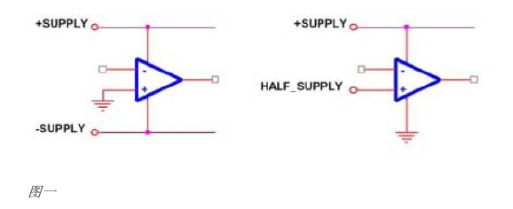

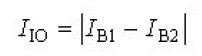
 The virtual short is because the voltage amplification of the ideal op amp is very large, and the op amp works in the linear region, it is a linear amplifying circuit, the output voltage does not exceed the linear range (that is, the finite value), so the non-inverting input of the op amp and the inverting input The potentials at the terminals are very close to equal. When the power supply voltage of the op amp is ±15V, the maximum output is generally 10~13V. Therefore, the voltage difference between the two input terminals of the op amp is below 1mV, which is approximately a short circuit between the two input terminals. This characteristic is called virtual short. Obviously, this is not a real short circuit, but a reasonable approximation within the allowable error range when analyzing the circuit. Since the input resistance of the op amp is generally more than a few hundred kiloohms, the current flowing into the non-inverting input terminal and the inverting input terminal of the op amp is very small, several orders of magnitude smaller than the current in the external circuit, and the current flowing into the op amp It can often be ignored. This is equivalent to an open circuit at the input of the op amp. This feature is called virtual disconnection. Obviously, the input terminal of the op amp cannot be truly open. Using the two concepts of "virtual short" and "virtual break", when analyzing the linear application circuit of the operational amplifier, the analysis process of the application circuit can be simplified. Operational circuits formed by operational amplifiers all require a certain functional relationship between input and output, so both conclusions can be applied. If the op amp does not work in the linear region, there will be no "virtual short" or "virtual break" characteristics. If the potential of the two input terminals of the op amp is measured and reaches a few millivolts or more, the op amp is often not working in the linear region or is damaged. Important indicators Input offset voltage UIO is an ideal integrated operational amplifier. When the input voltage is zero, the output voltage should also be zero (no zero adjustment device). But in fact, it is difficult for the differential input stage of the integrated operational amplifier to be completely symmetrical. Usually, there is a certain output voltage when the input voltage is zero. The input offset voltage refers to the compensation voltage added at the input to make the output voltage zero. In fact, it means that when the input voltage is zero, the output voltage is divided by the voltage amplification factor, and the value converted to the input is called the input offset voltage, that is, the size of UIO reflects the symmetry of the op amp and the potential coordination. The smaller the UIO, the better. Its magnitude is between 2mV and 20mV. The UIO of ultra-low offset and low-drift op amps generally has an input offset current between 1μV and 20μV. IIO. When the output voltage is zero, the differential pair of the differential input stage The difference between the quiescent current of the tube base is called the input offset current IIO, namely