How to measure the touch screen capacitance value in mass production
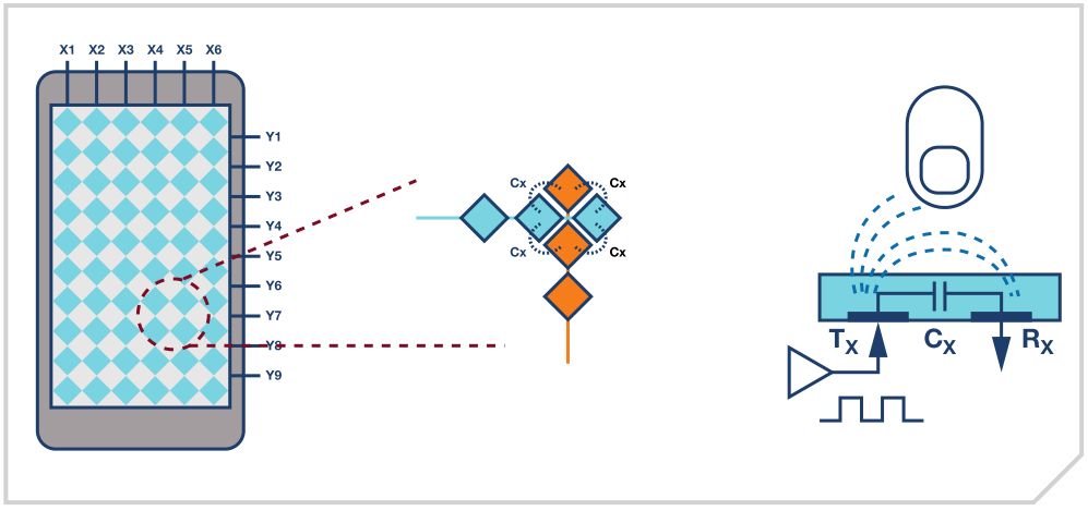
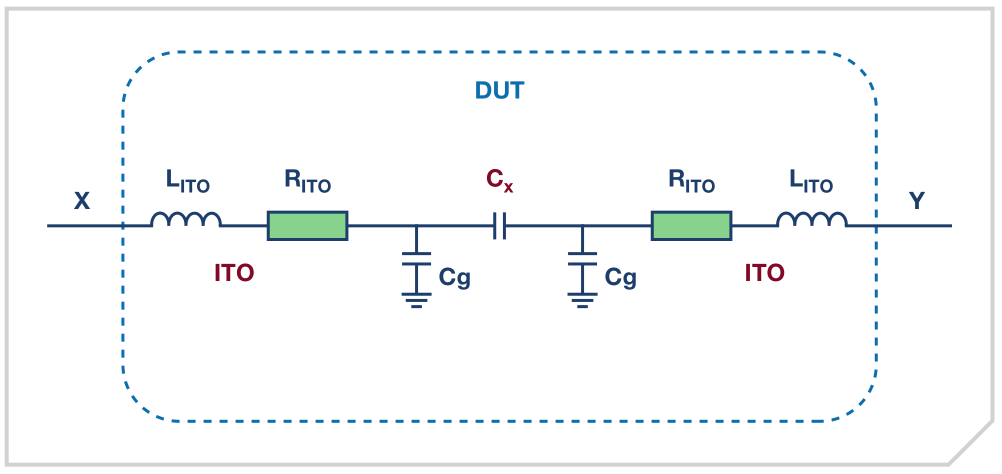
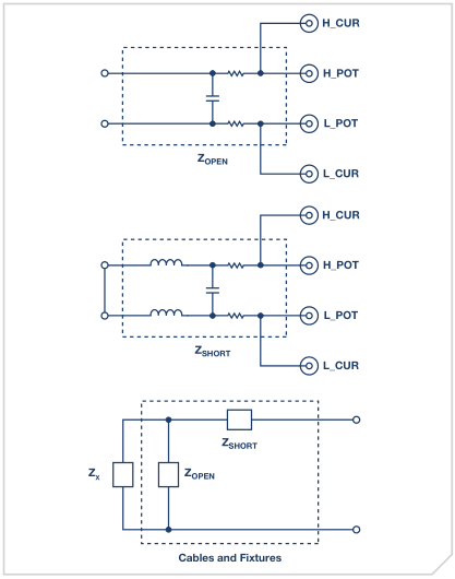
In addition, rapid testing and high sensitivity measurements are the two main goals in manufacturing testing. Relative accuracy in this application is more important than absolute precision. Increasingly demanding touch screen production, there is an urgent need for automated test solutions that can save a lot of time and labor costs. Touch screen technology Understanding touch screen technology can help you understand the test methods and system block diagrams in the next section. There are two main types of capacitive touch screen technology: self-contained screen and mutual capacitive screen , as shown in Figure 1. Figure 1. Two different types of touch screens In touch screen applications, mutual-capacity screens are more popular because the mutual-capacity screens can truly support multi-touch compared to self-contained screens. Figure 2. Mutual capacitance screen structure Most consumer-grade touch screens use ITO (Indium Tin Oxide) materials that are electrically conductive and light transmissive, with light transmissions typically greater than 90%. Figure 2 is one of the diamond-type mutual capacitance physical structures. The X column ITO and Y row ITO are on different layers, and the weak capacitance generated by their cross nodes is the mutual capacitance CX we want to measure. As the finger approaches it, as shown in the image to the right, the equivalent CX will decrease as the electric field changes. Let's create a DUT analysis model to get accurate measurements, as shown in Figure 3. 3. DUT analysis model CX : Each node is approximately 1 pF to 10 pF, which is the mutual capacitance we want to measure. There are hundreds to thousands of such mutual capacitance nodes that need to be measured. LITO : Parasitic inductance caused by ITO thin lines, 1 nH to 20 nH; we can ignore this in this application because its impedance is very low at less than 1 MHz. RITO : ITO wire resistance, kΩ level, depending on ITO wire length, wire width and material composition. The RITO of each node may be different. Cg : The parasitic capacitance relative to the reference level GND, pF level, which depends on the distance from the reference GND plane and the actual fixture environment in the factory. Production test requirements The solution involves 4 test projects: Single node capacitance test Measure all matrix nodes, approximately 10 pF or so; require high precision at the fF level. Adjacent row capacitance test A signal is applied to X1, measured from an adjacent X2; this is not a single node test, so measurements are typically on the order of tens to hundreds of pF. Open/short test of adjacent ITO lines During the manufacturing process, ITO diamond-type architectures sometimes cause short-circuits in adjacent lines, so this needs to be tested. ITO resistance ( optional ) This is an optional test item to evaluate whether the ITO line meets the standard. The test time for each node is usually at the ms level. The number of matrix nodes depends on the screen size, ranging from hundreds to thousands. ADI solution The test project involves different types of impedance (resistance and capacitance), so an impedance measurement device is required. This type of measurement can be done by a self-balancing bridge circuit, as shown in Figure 4. It consists of a circuit of known impedance (RTIA) and unknown impedance ZX. Unlike the proportional measurement of the conventional voltage division method, an active operational amplifier circuit A2 is used to control the voltage of the L_CUR point to maintain a constant potential (in this case, ground), and VS applies a fixed frequency signal to the H_CUR point. The opposite signal at the output of A2 is directly related to the current IX flowing through ZX. In order to avoid the effects of cable and switch parasitics, the second amplifier A1 is used to directly detect the voltage generated on the ZX. The waveforms generated by nodes POT and CUR represent the voltage and current signals on the measured impedance (ZX), respectively, so the impedance can be calculated by analog or digital methods. 4. Automatic balanced bridge for impedance measurement The unknown impedance ZX can be calculated using the formula: ZX = VPOT/VCUR × ZPATH Where VPOT is the voltage vector signal, VCUR is the current vector signal, and ZPATH is the total calibration coefficient of the overall gain and phase offset on the measurement path. For more information on impedance measurements, visit: http:// The touch screen test requirements can be realized by making some circuit supplements to the self-balancing bridge. As shown in Figure 5. Figure 5. Block diagram of the touch screen test system The signal excitation source is a high speed DAC or DDS that produces a 50 kHz to 200 kHz waveform for capacitance testing and ITO resistance testing. It also produces programmable DC voltage signals for open/short testing of adjacent lines. AMP1 has two roles in this circuit: differential to single-ended conversion and level shifting to dual supply signal mode. Amplitude adjustment can be done at the amplifier, DAC digital domain, or DDS full-scale control port. The voltage measurement path is implemented using a differential input amplifier, AMP3, and is digitally sampled by a SAR ADC. The current measurement path consists of a programmable gain impedance amplifier (for converting current to voltage) and an additional amplifier AMP5 (for adjusting gain). Note that the switch configuration used to implement the programmable gain impedance amplifier must be carefully considered to minimize the effects of parasitic effects2. The signals in both measurement paths require level shifting and single-ended to differential conversion through AMP6 and AMP7 to meet the needs of the ADC input. For the ITO open/short test , since all measurement paths are DC coupled, it is only necessary to apply one DC signal to one line and then measure the loop current from the adjacent line. If this current is greater than the preset threshold, it means that the two lines are shorted. The ITO resistor can only be measured by the coupling between the nodes, so a sine wave needs to be applied to obtain its value and measure the capacitive node. The benefit of using a high-resolution SAR ADC is that there is no need for phase and amplitude detection of the analog domain, which can be done by a processor or FPGA for greater flexibility and better performance. Of course, it is also possible to use only one ADC to multiplex the measurement path with SW1/SW2, but the disadvantage is that the test time will increase. Considering hundreds of channel connections, we recommend using analog switches here, which saves a lot of space and shortens the signal path length. In order to understand its impact on the measurement, it is necessary to analyze the parasitic effects of the switch. Therefore, two switches should be added as shown in Figure 6 for analysis. 6. Analog switch analysis model CD/CS : Parasitic capacitance, 8 pF to 32 pF (ADG1414), the capacitance is different in both on and off states. The matrix node test will connect a large number of switches, so we have to consider the sum of this parasitic capacitance. CDS : Parasitic capacitance with a shutdown state isolation of –73 dB (ADG1414) at 1 MHz, so this application can be ignored. For conduction, we can also ignore it because RON is much lower than ZCDS. RON : The on-resistance RON of the analog switch is 9.5 Ω when using the ADG1414. The effect of this resistance on the measurement path can be eliminated with an appropriate Kelvin connection, but it is still on the signal path and therefore needs to be considered. CP : Other parasitic capacitance on the board, pF level, is not the biggest problem. These parasitic effects need to be measured before testing the touch screen to account for its effect on the total capacitance and resistance on the measurement path. The compensation procedure involves two measurements: open circuit and short circuit compensation. The open circuit compensation procedure is to perform impedance measurement when the cable and fixture are connected to the measurement circuit but disconnected from the object to be tested; Short-circuit compensation is the connection of all terminals through a test fixture and then impedance measurements. This compensation can be done using the analog switch used in touch screen measurements . The equivalent circuit of these two compensation procedures is shown in Figure 7. 7. Compensation for test fixture parasitics The diagram to the right shows the complete network model derived from the open and short circuit compensation procedures. After knowing the open circuit and short circuit impedance values ​​ZOPEN and ZSHORT, the value of the unknown impedance ZX can be found by the following equation. ZX = ZOPEN × (ZM – ZSHORT)/(ZSHORT + ZOPEN – ZM) Where ZM is the impedance measured for this system. High measurement speed: If the signal uses 100 kHz as complete a single node capacitance touch screen project test (assuming a total of 512 nodes) from about 5 ms to 10 ms. This does not include path switching and other setup times. If you consider more test items and communications, a DUT will take approximately 500 ms to 2000 ms, depending on the actual environment and how many measurements need to be averaged to achieve stable results. High sensitivity: With an 18-bit ADC, the resolution is less than 10 fF, and the accuracy of a 1 pF DUT is about 1% to 5%; the accuracy depends on the actual environment and design.
ZGAR TWISTER Disposable
ZGAR electronic cigarette uses high-tech R&D, food grade disposable pod device and high-quality raw material. All package designs are Original IP. Our designer team is from Hong Kong. We have very high requirements for product quality, flavors taste and packaging design. The E-liquid is imported, materials are food grade, and assembly plant is medical-grade dust-free workshops.
Our products include disposable e-cigarettes, rechargeable e-cigarettes, rechargreable disposable vape pen, and various of flavors of cigarette cartridges. From 600puffs to 5000puffs, ZGAR bar Disposable offer high-tech R&D, E-cigarette improves battery capacity, We offer various of flavors and support customization. And printing designs can be customized. We have our own professional team and competitive quotations for any OEM or ODM works.
We supply OEM rechargeable disposable vape pen,OEM disposable electronic cigarette,ODM disposable vape pen,ODM disposable electronic cigarette,OEM/ODM vape pen e-cigarette,OEM/ODM atomizer device.
ZGAR TWISTER Vape,ZGAR TWISTER Vape disposable electronic cigarette,ZGAR TWISTER Vape pen atomizer ,ZGAR TWISTER Vape E-cig,TWISTER Vape disposable electronic cigarette Zgar International (M) SDN BHD , https://www.zgarette.com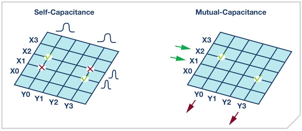
 Impedance measurement
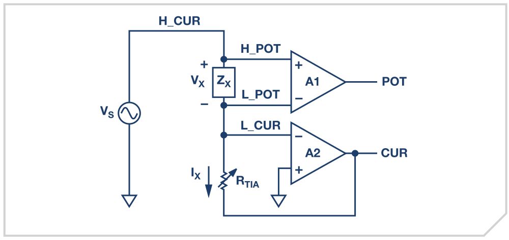
 Touch screen test system block diagram
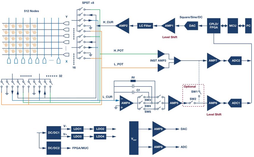
 Interface with the measured touch screen
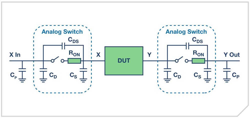
 Two main indicators

