Application Analysis of Highly Integrated RF Front End Module Supporting Long Distance Bluetooth Communication
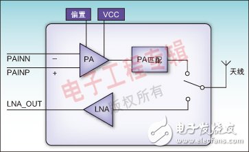
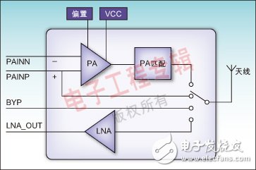
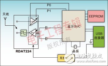
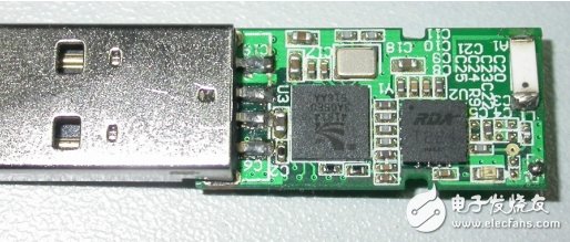
Bluetooth communication is a time division multiplexing (TDD) technology operating in the 2.4 GHz to 2.48 GHz band, designed to replace cables to connect portable and / or fixed equipment, and to ensure a high degree of security. The main features of Bluetooth technology are powerful, low power consumption, low cost, and can handle both data and voice transmission. Depending on the transmit output power, Bluetooth transmission has three distance classes: Class1 is about 100 meters; Class2 is about 10 meters; Class3 is about 2 to 3 meters. For long-distance Bluetooth technology applications, RADICO Microelectronics has introduced the RDAT224 and RDAT212 RF front-end module chips. The RDAT224 chip integrates a power amplifier (PA), a low noise amplifier (LNA) and a T/R RF switch. The input and output of the chip have been matched to 50Ω inside the module. The package is made of LGA suitable for RF module design, and its size is only 5 & TImes; 5mm2, which is very suitable for USB Dongle Class1 product design. The RDAT212 chip also integrates PA, LNA and antenna switches, and specifically increases the power-saving features of PA bypass and LNA bypass. The input and output of the chip have been matched to 50Ω inside the module, and the product size is further reduced to 3&TImes; 3mm2. The advantages of power saving and small size make the RDAT212 chip suitable for mobile phone Bluetooth and 802.11.b/g expansion applications in the future. At the same time, both products have good linearity and support high-speed applications of Bluetooth 2.0. The PA and LNA integrated in the RDAT224 RF front-end module are fabricated using an advanced GaAs Heterojunction Bipolar Transistor (GaAs HBT) process, and the T/R RF switch uses an enhanced high electron mobility field effect transistor (E-PHEMT). Process manufacturing. Although not in the form of a differential PA, the RDAT224 still provides a differential input pin, eliminating the need for the user to care about the differential-to-single-ended design. The PA has a gain of 20dB in the 2.4GHz~2.5GHz band. Thus, the RDAT224 module can provide 20dBm output power under 0dBm input conditions, meeting Class1 power output requirements. The power-added efficiency of the PA at 21dBm output is as high as 40%, which helps to extend the power supply time. The LNA has a gain of 15dB in the 2.4GHz~2.5GHz band, a static operating current of only 9mA, a noise figure of less than 3dB, and an input third-order intercept point IIP3 of -5dBm. The input and output of the module have been internally matched to 50Ω, and the customer application does not need to design matching circuits on the PCB, making PCB design easier. The output harmonics of the PA have been suppressed to below -50dBc, and the filter is usually not required externally when applied. In this way, only a small amount of filter capacitor is needed outside the module, which greatly reduces the PCB size and reduces the system cost. RDAT212 adds power-saving features for PA bypass and LNA bypass. In Class1 applications, the module can provide 20dBm of output power at 0dBm input; in Class 2 applications, the module can be switched to the PA bypass state without consuming current. Figure 1: Schematic diagram of the internal structure of RDAT224 Figure 2: Schematic diagram of the internal structure of RDAT212. The LNA uses the E-PHEMT process to further reduce the noise figure and increase linearity. The LNA has a gain of 13dB in the 2.4GHz~2.5GHz band, a static operating current of only 5mA, a noise figure of less than 2dB, and an input third-order intercept point IIP3 of up to 8dBm. The LNA bypass function can be used both as a power saving mode and as a dynamic range of the receiver. The input and output of the RDAT212 have been internally matched to 50Ω, and a harmonic suppression circuit is integrated inside the chip. The original Bluetooth design consisted of a series of separate ICs and support circuits and eventually formed a Bluetooth module. As technology advances, the integration of Bluetooth designs continues to increase while external devices continue to decrease. Figure 3: System schematic of a Bluetooth adapter design. Figure 3 shows a modular solution with the RDAT224 chip as the RF front-end module and a Bluetooth SoC as the baseband. The SoC is directly connected to a device such as a PC through a USB connector, completes the baseband function, and upconverts the signal into a radio frequency signal to the T224 radio front-end module, and simultaneously provides a control interface of the T/R radio switch, PA, and LNA. The RDAT224 RF front-end module amplifies the RF signal and transmits the signal to the antenna via an RF switch. The RDAT224's PA provides 20dBm of output, allowing the Bluetooth adapter to have an effective range of up to 100 meters. When the Bluetooth adapter receives the signal, the RF signal is transmitted to the LNA via the RF switch. The LNA noise figure of RDAT224 is less than 3dB, which can greatly improve the sensitivity of the receiving link. The RF signal is amplified by the LNA and then down-converted by the SoC, and transmitted to the PC and other devices by the USB connector. The RDAT224 RF front-end module integrates the T/R RF switch, PA and LNA, greatly reducing the complexity of the Bluetooth module. If designers don't use the highly integrated modules described above, they must design the Bluetooth PCB very tightly. Component placement, tracking scanning, decoupling, grounding, shielding, and boarding are all important factors that affect performance, especially the RF performance of the product. If RDAT224 is used, the designer will be able to circumvent these issues so that there is no need to pay special attention to the above factors in the final design. In addition, RDAT224 can also help reduce PCB size and further reduce costs. Figure 4 shows a PCB photo of the Bluetooth adapter. It can be seen that the area is small, except that the RDAT224 chip and the Bluetooth SoC chip have few external components. Figure 4: PCB physical map of the Bluetooth adapter Plastic Bluetooth Charger,Mobile Charger Wireless,Suction Cup Wireless Power Bank,Suction Power Bank Shenzhen Konchang Electronic Technology Co.,Ltd , https://www.konchang.com