PCB wiring tips introduced by old engineers
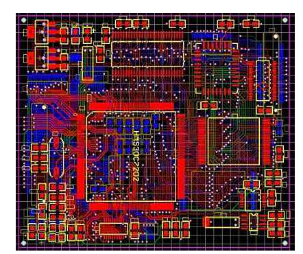
PCB, also known as Printed Circuit Board, enables line connection and functional realization between electronic components and is an important part of power circuit design. This article will introduce the basic rules of PCB board layout and wiring today. First, the basic rules of component layout 1. According to the circuit module layout, the related circuit that realizes the same function is called a module, and the components in the circuit module should adopt the principle of near concentration, and the digital circuit and the analog circuit are separated; 2. Positioning holes, standard holes, etc. shall not be placed within 1.27mm around the mounting holes. Components such as components and screws shall not be placed around 3.5mm (for M2.5) and 4mm (for M3) mounting holes. 3. Avoid the over-holes under the components such as the horizontal resistors, inductors (inserts), and electrolytic capacitors to avoid short-circuiting the vias and component housings after wave soldering; 4. The distance between the outer side of the component and the edge of the board is 5mm; 5. The outer side of the mounting component pad and the outer side of the adjacent interposing component are greater than 2 mm; 6. Metal shell components and metal parts (shield boxes, etc.) cannot be in contact with other components, and should not be in close contact with the printed wires or pads. The spacing should be greater than 2mm. The positioning hole, the fastener mounting hole, the elliptical hole and the outer side of the other hole in the plate are larger than 3 mm; 7. The heating element cannot be in close proximity to the wire and the heat-sensitive element; the high-heat device should be evenly distributed; 8. The power socket should be placed around the printed circuit board as much as possible. The power socket and the bus bar terminal connected to it should be placed on the same side. Special care should be taken not to place power outlets and other solder Connectors between the connectors to facilitate soldering and Power Cable design and cable ties for these sockets, connectors. The spacing between the power socket and the soldering connector should be considered to facilitate the insertion and removal of the power plug; 9. Arrangement of other components: All IC components are unilaterally aligned, and the polarity of the polar components is clearly marked. The polarity on the same printed board shall not be more than two directions. When two directions are present, the two directions are perpendicular to each other; 10, the board surface wiring should be properly dense, when the difference between the density is too large, it should be filled with mesh copper foil, the grid is larger than 8mil (or 0.2mm); 11. There should be no through holes on the chip pads to avoid solder joint loss and solder joints. Important signal lines are not allowed to pass between the socket feet; 12, the patch is unilaterally aligned, the characters are in the same direction, and the package direction is consistent; 13. Polarized devices should be as consistent as possible in the direction indicated by the polarity on the same board. Second, the component wiring rules 1. Draw wiring in the area where the wiring area is ≤1mm from the edge of the PCB board and within 1mm around the mounting hole. 2, the power cord should be as wide as possible, should not be lower than 18mil; signal line width should not be lower than 12mil; cpu input and output should not be lower than 10mil (or 8mil); line spacing is not less than 10mil; 3, the normal through hole is not less than 30mil; 4, double in-line: pad 60mil, aperture 40mil; 1/4W resistor: 51*55mil (0805 surface mount); pad 62lu when in-line, aperture 42mil; Infinite capacitance: 51*55mil (0805 surface mount); pad 50mil in line, aperture 28mil; 5. Note that the power and ground lines should be as radial as possible, and the signal lines should not have loopback traces. How to improve anti-interference ability and electromagnetic compatibility? How to improve anti-interference ability and electromagnetic compatibility when developing electronic products with processors? 1, the following systems should pay special attention to anti-electromagnetic interference: (1) A system with a particularly high clock frequency and a particularly fast bus cycle. (2) The system contains high-power, high-current drive circuits, such as spark-generating relays, high-current switches, and so on. (3) A system containing a weak analog signal circuit and a high-precision A/D conversion circuit. Our
company offers rubber, and specialty seal and o-ring for molding electronic and electrical connectors, both circular
and rectangular types. We have in house capabilities and quick turn
around.
Cable Grommets with various Grommet Shapes, Rib Styles, Slot Shapes, Inner Flanges,
and Colors - To have access to our 3D Cable Grommet Design Tool
Silicone Rubber Products,Cable Silicone O-Ring,Rubber Seal,Custom Silicone Seal,Waterproofing O-Ring,Tpe Grommet ETOP WIREHARNESS LIMITED , https://www.wireharnessetop.com