Design, implementation and verification of MMIC for RF front-end module in 28GHz 5G communication band
As the 5G millimeter wave is expected to enter commercial use, the research and development of key companies in the industry is progressing smoothly, and the specification, design and verification of customized component indicators have been completed. The basic component required to implement a future millimeter-wave 5G system is the RF Front End Module (FEM). The module includes the final amplifier stage of the transmitter and the front-end amplification stage and the transmit/receive switch (Tx/Rx) in the receiver to support Time Division Duplex (TDD). The FEM must have high linearity in transmit mode and a low noise figure in receive mode. Since the millimeter wave 5G system may require the user terminal to use multiple FEMs to form a phased array architecture or a switched antenna beam architecture. Therefore, FEM must be implemented in an efficient, compact and cost-effective manner, and is preferably simple to control and monitor.
This paper introduces the design, implementation and verification of the RF front-end module MMIC (single-chip microwave integrated circuit) in the 28GHz 5G communication band (27.5 to 28.35GHz) that meets all the above requirements. The RF front-end was developed by Plextek RFI and implemented using WINSemiconductors' PE-15 4V voltage, 0.15μm, and enhanced GaAs PHEMT process. It is available in a compact, low-cost, SMT (surface mount)-compatible 5mm x 5mm overmolded QFN package for high volume, low cost manufacturing. It covers 27 to 29 GHz and therefore supports the full 28 GHz 5G band.
Design goal
The design of the FEM transmit channel focuses on achieving high efficiency under power retraction to provide linear amplification, which is a requirement of the 5G communication system. The target power added efficiency (PAE) under power retraction is set at 6%, and the third-order intermodulation (IMD3) is lower than -35 dBc (power back-off value: approximately 7 dB is returned from the 1 dB compression point). The RF output power corresponding to the 1 dB compression point (P1dB) is set to 20 dBm. The receive channel needs to achieve a noise figure of less than 4dB (including switching losses) at very low current consumption (maximum 15mA, +4V supply).
The functional block diagram of the RF front-end MMIC is shown in Figure 1. The transmit signal path extends from the left to the right in the upper half of the figure; the input port is on the pin labeled "PA_RFin". The input signal is amplified by a three-stage power amplifier (PA) and then connected to the antenna via an RF power detector and a single pole double throw (SPDT) switch. An on-chip directional power detector monitors the transmitted RF output power and integrates temperature compensation on-chip. The compensated power detector output is determined by the difference between the voltage "Vref" and the voltage "Vdet". A fast switch enable circuit (PA enable circuit in Figure 1) controlled by an (active low) logic signal "PA_ON" is integrated into the chip. The PA can be powered up and down quickly when switching between transmit and receive modes, thereby achieving a current of only 0.1 mA when the PA is not in use, maximizing the efficiency of the overall system.
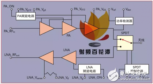
Figure 1: Functional block diagram of a 28GHz 5G communication RF front-end module chip
The PA typically operates at a factor of a few dB back from the compression point to keep the modulated signal it emits from being severely distorted. The design method is to optimize the performance of the power amplifier operating at about 7dB back-off at the P1dB point. In order to achieve a better PAE under this operating condition, the PA will be biased in the deep AB class.
2. Design compromise strategy
The design begins with device level simulation of candidate cell transistors. This simulation provides key information such as device size, bias point, target impedance, PA level, and driver ratio, laying a solid foundation for subsequent fine power amplifier designs.
An important part of this work is to determine how to maximize the PAE under power back-off. In general, this can be achieved by reducing the device's static bias current density. However, the range in which the current density can be down-regulated in this method is limited by the gain and linearity constraints, as both deteriorate as the current density decreases. There is a clear compromise between PAE and gain and linearity under power back-off conditions.
The linearity indicator of primary interest in the design is that under power back conditions, IMD3 must be less than -35dBc. As shown in Figure 2, IMD3 performance is particularly sensitive to fundamental frequency loading conditions with reduced bias current. Figure 2a shows the load pull simulation results for 8&TImes biased to deep AB; 50μm devices at 4V, 75mA/mm, and the load corresponding to the PAE optimum point at P1dB. The figure also shows the performance of IMD3 under the optimal load and power back-off conditions simulated, showing that there is a margin of about 4 dB from the -35 dBc indicator. The simulated PAE is approximately 15% under this power backoff condition, and this efficiency is only factored into the device and does not include any output loss. Figure 2b shows the load corresponding to the P1dB power optimum point and the IMD3 information under the same device and bias operating conditions. It is found that the performance of IMD3 is significantly worse under the same relative power retreat, exceeding the target by more than 5 dB, and the PAE is similar to the former condition, which is about 15.7%.
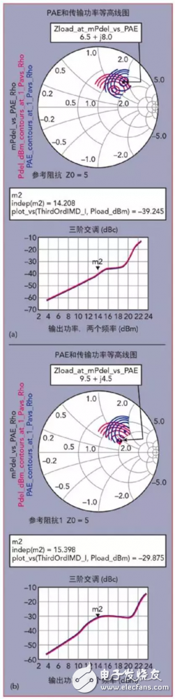
Figure 2: Impedance point corresponding to the best PAE under P1dB condition and IMD3(a) under the corresponding power back-off condition; impedance point corresponding to the optimal power under P1dB condition and IMD3(b) under the corresponding power back-off condition .
Further evaluation of the performance of the power amplifier under both P1dB and power back-off conditions at other impedance points on the Smith chart. The load conditions in Figure 2a clearly have the best overall performance and are therefore chosen for the output stage design. Finally, a bias current of 52 mA/mm was selected, and an 8x50 μm device was selected as the basic unit of the output stage to meet the power specification requirements. According to the total transmission gain index, it is determined that three-stage amplification is required.
A complete three-stage power amplifier is designed by sequentially selecting the optimum transistor size for the drive amplifier stage and the pre-drive amplifier stage. This also requires careful consideration of design compromises because larger transistor sizes improve overall linearity but reduce PAE. When the size and bias of all transistors are determined, the detailed design of the matching and biasing circuits can continue. Layout design needs to be considered from the early stages of the design process to avoid introducing excessive parasitic effects and ensuring design achievability. The first and second stages of the amplifier use a common gate bias lead (added on pin PA_Vg12), while the third stage sets a separate bias lead (PA_Vg3). This allows the two voltages to be individually optimized to improve the linearity or PAE of the PA. The drain supply can similarly apply +4V across two separate pins on "PA_Vd12" and "PA_Vd3", although the two pins are connected on the PCB.
The SPDT switch uses a serial-to-parallel structure in which multiple transistors are integrated in the series and parallel branches to improve linearity1. The capacitance of the transistor when it is turned off limits the inherent isolation of the device at high frequencies in the off state, and the isolation of the switching transistor is only a few dB2 at 28 GHz. Reducing the transistor size improves the inherent isolation, but increases the insertion loss and reduces the linearity in the on state, so it is not a viable option. The approach taken here is to use on-chip inductor compensation to improve the isolation state of the off state. The careful design ensures low insertion loss in the on-state to achieve high output power of the transmit channel and low noise figure of the receive channel. The switch is controlled by a bit control voltage "Vctrl1", which is set to 4V for the transmit mode and 0V for the receive mode. The "single pole double throw control circuit" (SPDT control circuit) enables single bit control, which is essentially a one-to-two-wire decoder. The total current consumed by the control circuit and the SPDT itself is only 1 mA, provided by the +4V supply applied at "VD_SW".
The input to the receive channel is located at the "antenna" pin that is connected to the two-stage LNA input via the SPDT. The output of the receive channel is located on the pin labeled "LNA_RFout". Like the PA, the LNA also has a fast switching enable circuit that allows the LNA to consume only as little as 0.1mA when not in operation. The key to the low noise amplifier design process is to find a design that consumes low current, good noise figure, and sufficient linearity.
The important first step is to choose the right transistor size. Multiple short fingers can be used to reduce the gate resistance of the transistor and improve the noise figure. The two stages of the low noise amplifier use series inductive feedback so that the impedance required for the best noise figure is closer to the impedance required for conjugate matching and optimum gain.
The first stage of the low noise amplifier is designed with noise figure as the optimization target, but still needs to generate enough gain to fully reduce the influence of the second stage noise figure. The noise figure of the second stage of low noise is not important, so this stage is designed to have a higher gain than the first stage. The designed LNA requires only 10 mA of DC current from a +4V supply. The gate bias voltage is applied to pin "LNA_Vg" and the +4V drain bias voltage is applied to "LNA_Vd". The “LNA_Vsense†pin provides monitoring of the bias current. The monitored bias current information can be used to control the gate voltage to compensate for changes in environmental conditions such as temperature. At the correct bias, the voltage at this monitor pin is 3.9V. The process of using enhanced transistors means that only a positive supply voltage is required, making the MMIC very easy to integrate.
Careful electromagnetic simulation is very important to ensure good RF performance of each module. A step-by-step approach was used to add a portion of the circuit to the EM simulation each time, while the rest was still modeled using the model in the Process Design Kit (PDK). Since integrated circuits are used in plastic packages obtained by overmolding processes, compounds injected over integrated circuits also need to be considered in electromagnetic simulation.
3. Evaluation and testing
Figure 3 is a photograph of a radio frequency front end chip. The RF front-end MMIC chip size is 3.38mm &TImes; 1.99mm. The pad/pin location is similar to that shown in the block diagram, and it also integrates multiple ground pads to make it fully RF-ready. It is designed for low cost injection molding in 5mm & TImes; 5mm QFN packages. And considering the influence of the mold plastic, it is necessary to carefully design the RF transition interface from the chip to the PCB. A custom lead frame is designed to achieve this transition, and the RF ports on the package are designed as ground-signal-ground (GSG) interfaces.
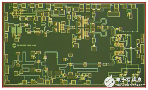
Figure 3: Chip photo of the 28GHz 5G communication RF front-end module MMIC
After the fabrication and fabrication, the on-chip RF test was performed on multiple chips to confirm that the chip achieved a successful design goal before the package. The RF test results are not given here. All the results given are measured after the chip is fully packaged and mounted on a typical PCB evaluation board.
A10 600 Puffs,A10 600 Puffs Box,A10 600 Puffs Disposable,A10 600 Puffs Disposable Vape
Lensen Electronics Co., Ltd , https://www.lensenvape.com