Talking about Altium's five major functions
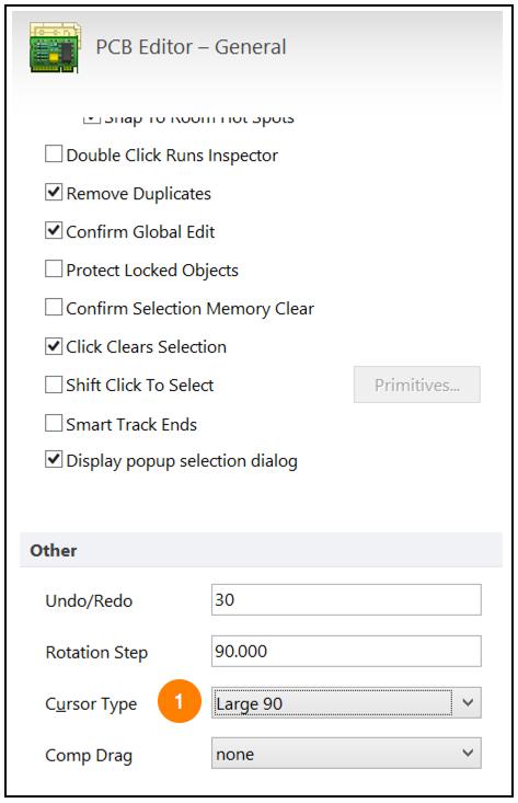
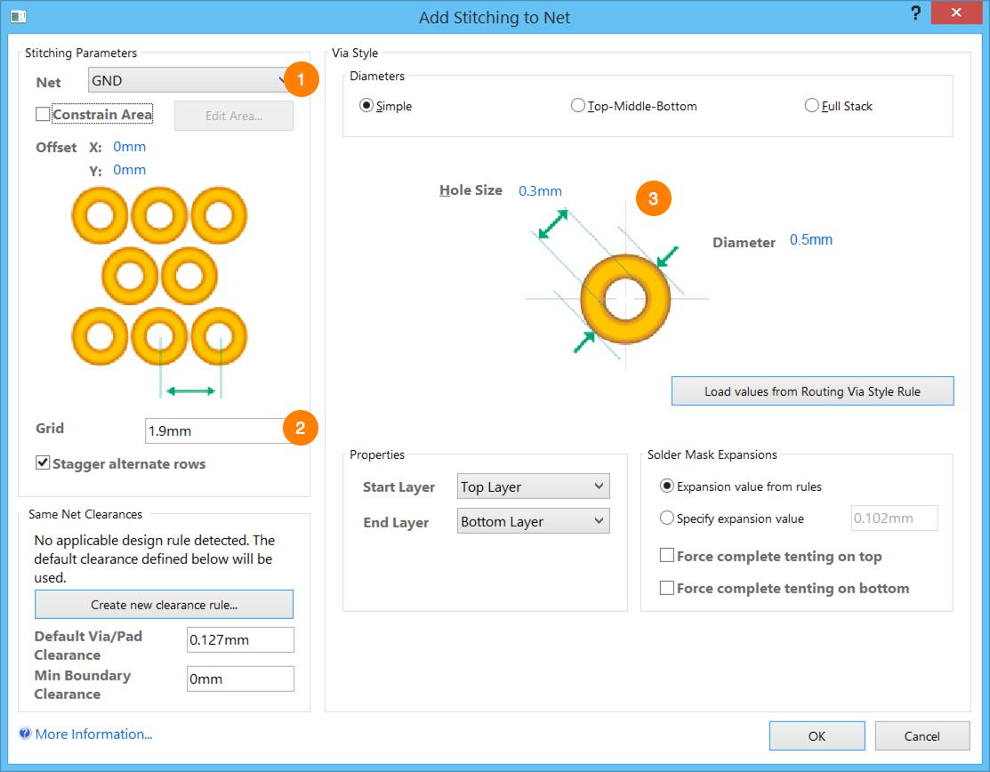
I communicated with many excellent engineers who are proficient in AlTium. They devoted countless hours and energy to learning, using, and developing AlTIum Designer. Why is AlTIum so attractive? Let me summarize the five most effective features they use in the design process every day. Do you also benefit from these features? Read it carefully to find out. Insert element pin data automatically using Smart Grid Insertion The component creation process can be very time consuming, especially for multi-pin components. AlTIum Designer's smart grid insertion feature is easy to use and can help you import existing tabular data into Altium Designer without having to spend a lot of time on component pin creation. This feature is very effective in saving time and efficiency. Suppose you need to create a 1000-pin component in Altium Designer. To simplify the process, you can: In this example, I created a 44-pin component. To use the Smart Grid Insert feature, we need two additional files: If your spreadsheet has defined the format of all pin configuration data, you can import it to Altium Designer in the following steps: 1. In the lower right corner of the workspace, select SCH > SCHLIB List . 2. Right-click in the SCHLIB List window and select Smart Grid Insert . ( Note: If Smart Grid Insert cannot be selected, make sure it is in edit mode.) 3. In the new spreadsheet data window that opens, select Automatically Determine Paste > OK (Figure 1). Automatically add pin data using Smart Grid Insertion Now that all the pins are automatically positioned, you can add a rectangular box and link the pins to complete the component creation process. Watch the video below to learn how to quickly create components with smart grid insertion. Select a row of vias by selecting The Select option is a highly productive enhancement that allows you to navigate to a specific object in your design and then modify its properties in the Inspector panel. Just want to select a specific group of vias? Or, just want to select the connection associated with a particular component? You can do more with Altium Designer's touch selection feature. In this example, I use the Touching Line option to select a row of vias. Because they are very close to other vias and traces on the board, using a standard rectangle does not accurately select them. To select these objects: 1. Enter the keyboard shortcuts S , L to activate the contact selection command. 2. Left-click on the board and start selecting. 3. Drag the selection line to the desired selected object and left-click again to confirm. The object you select will be highlighted on the board. In our example, simply open the PCB Inspector panel and change the diameter of the selected via. I suggest that you browse all the command options (shortcut: S) in the Select menu. Depending on your design needs, specific selection patterns may be required. Large cursor options in Altium Designer Have you always suffered from the precise positioning of components and wires? A large cursor can help you place components, wires, and other design objects precisely, making it easier and more efficient to operate. Relative to using a small cursor, a large cursor can significantly improve your efficiency, and a small cursor can only extend the cross cursor when placing an object within a small distance. You can configure Altium Designer's cursor type, including several available options (Small 45, Small 90, and Large 90), and we strongly recommend that you choose Large 90 in your board layout to maximize your productivity. To activate this setting in Altium Designer: 1. In the upper left corner of Altium Designer, select DXP > Â Preferences. 2. In the left navigation bar, select the PCB editor - General page. 3. In the Other area, change the cursor type to Large 90 (Figure 1). 4. Click Apply to save the settings. Cursor type options in DXP Preferences Now that the cursor has grown in size, select a component or wire in your PCB design and try to move it. You will find that the horizontal and vertical cross cursors extend to the edge of the visible window, allowing you to place objects more precisely than before. Copy objects in a schematic design There are many duplicate designs in the schematic design. In fact, you don't need to fetch the same object from the library every time. There is a quick and simple function that can help you to copy the existing object and then place it on the schematic. This way, you can save a lot of time when you run into the problem of schematic object placement, without any additional adjustments. The copy object function is very easy to use, and does not require any settings. In the example, we want to add decoupling capacitors to the schematic design. To copy this object on the schematic: 1. Hold down the Shift key and left-click to select and drag the copied element to the target position. Once the mouse is released, the newly copied symbol is placed in the design and all original object parameters are preserved. You can copy the same object as you like, or use different selection tools to select multiple objects at once and copy them. Add stitched holes to the selected network Through-hole stitching can save a lot of time and increase productivity. It can help you quickly create a via grid on the circuit board copper for connecting different copper layers. If you are looking for a simple and effective way to create a tight electrical connection and create a better cooling path between the layers of the PCB design, then via stitching is your best choice. In this example, I have a grounded network on the PCB and I want to add stitched vias to it. First, you need to open the PCB document: 1. Select Tools> Via Stitching/Shielding> Add Stitching to Net 2. Select the network where you want to stitch the vias (Figure 1). In our example, the GND network was selected. 3. In the Grid field, enter the desired via spacing. (figure 2) 4. Adjust via size and diameter as needed . (image 3) 5. Select OK to complete the setup. Set up stitching With this setting applied, the grid-based array of vias is immediately added to the network you specify, as shown in the following figure. We have been working hard to further increase productivity in each new release of Altium Designer. In the coming weeks, we are very happy to share with you a series of latest updates. In the coming week, we will introduce five other acclaimed feature features!
Small computer system interface (SCSI) is an independent processor standard for system level interfaces between computers and intelligent devices (hard disks, floppy drives, optical drives, printers, scanners, etc.). SCSI is an intelligent universal interface standard.
In addition to SCSI, IDE is also a very common interface. From the point of view of ease of use, IDE is more suitable for ordinary users. In addition, personal computer users not only need to configure a few peripherals, but also do not require high speed. Therefore, it is more appropriate to choose IDE interface. In addition, IDE also has the characteristics of high performance price ratio and wide application. Although the SCSI interface has many incomparable characteristics, the price of the interface and its peripherals is too expensive to be borne by ordinary users, which determines the limitation of its actual use range. SCSI Solder Type Section ShenZhen Antenk Electronics Co,Ltd , https://www.antenk.com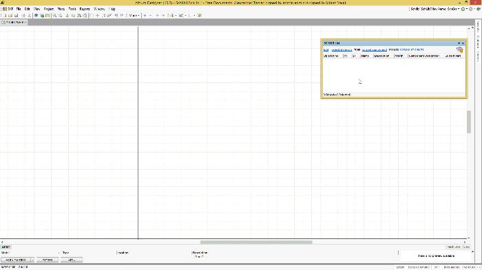
1. The working mode of IDE requires the whole process participation of CPU. When the CPU reads and writes data, it can't perform other operations. In this case, in the multitask operating system of Windows 95 / NT, the system reaction will be greatly slowed down. The SCSI interface controls the data reading and writing operation completely through the independent high-speed SCSI card, so the CPU does not have to waste time to wait, which obviously can improve the overall performance of the system. However, IDE interface has also made great improvements to improve this problem. DMA mode can be used instead of PIO mode to read and write data. DMA channel is responsible for data exchange, which greatly reduces the CPU consumption. However, comparing the CPU utilization of SCSI and IDE, we can find that SCSI still has considerable advantages.
2. The scalability of SCSI is larger than that of IDE. Generally, each ide system can have two IDE channels, with a total of four IDE devices. The SCSI interface can connect 7-15 devices, much more than IDE, and the cable connected is far longer than ide.
3. Although the price of SCSI device is higher, compared with IDE, the performance of SCSI is more stable, durable and reliable.